

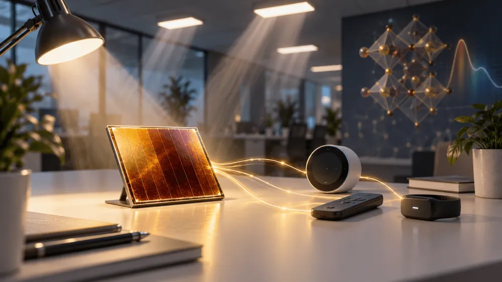
The light from LED ceiling fixtures and desk lamps in offices is far weaker than direct outdoor sunlight, and its energy is concentrated in a narrower band of wavelengths. Technology that could power sensors and small devices for extended periods using only indoor light—similar to the tiny light-receiving surface on a calculator—has long been anticipated, but conventional silicon solar cells struggle to generate sufficient voltage and output under such conditions. Simply bringing a semiconductor designed for outdoor sunlight into a dimly lit room does not yield high conversion efficiency.
A joint research team including Penn State University fabricated a perovskite solar cell specifically tailored for indoor light by adjusting the halogen composition within the crystal structure. According to a peer-reviewed open-access paper published in the academic journal APL Energy on September 1, 2026 (DOI: 10.1063/5.0337271), a thin-film device with a bromine ratio adjusted to 35% recorded an indoor photovoltaic conversion efficiency (PCE(i)) of 36.2% under 1,000-lux white LED illumination. This figure was obtained from an extremely small test cell with an active area of just 0.093 square centimeters.
The key scientific achievement lies in how the team suppressed phase segregation—a longstanding problem in which increasing bromine content tends to cause the crystal to separate internally into iodine-rich and bromine-rich regions, reducing stability—through a surface protective layer formed with a specific organic salt. However, the projection of "operational lifetimes of several thousand hours" mentioned in the research announcement is an extrapolation based on just over 200 hours of laboratory data, not a confirmed result of actual continuous operation over thousands of hours. Assessing the practical viability of this technology requires separating the headline efficiency figure from both the specific measurement conditions and the material limitations revealed by thermal testing.
The Measurement Conditions Behind 36.2% on a 0.093 cm² Micro-Cell
Solar cell performance is typically evaluated using a light source that simulates the standard terrestrial solar spectrum (AM 1.5G, irradiance of 100 mW/cm²). In indoor photovoltaics (IPV) research, however, measurement conditions such as illuminance and light source spectrum have not been consistently standardized for many years. Even with identical materials, reported conversion efficiencies can vary significantly depending on the color temperature of the LED used and the mask aperture area during measurement.
The research group behind this study, led by Ivy M. Asuo and Nutifafa Y. Doumon of Penn State's Department of Materials Science and Engineering and the university's Materials Research Institute, also included researchers from North Carolina Central University. The figures reported by the team are based on measurements from a clearly defined small-area cell.
Under 1,000-lux white LED illumination, the developed device achieved a maximum power density of 112.2 microwatts per square centimeter (), a fill factor (FF) of 76.5%, an open-circuit voltage (Voc) of 1.04 volts, and a short-circuit current density (Jsc) of 141.28 microamperes per square centimeter ().
The active area used in this measurement was 0.093 square centimeters—smaller than a square with sides of about 3 millimeters. This is vastly different in scale from the modules of several square centimeters or more found in commercial electronics, or the large panels integrated into building materials. Small-area cells are less susceptible to variations in film thickness and localized crystal defects, and the effects of electrode resistance are also minimized, making it easier to achieve higher efficiency than with larger-area modules.
データを表で見る
| 35Br device (DCB+PEABr) (Value) | |
|---|---|
| Short-circuit current density (µA/cm²) | 141.28 |
| Open-circuit voltage (units of 10 mV) | 104 |
| Fill factor (%) | 76.5 |
| Conversion efficiency (%) | 36.2 |
As the bar chart shows, because short-circuit current density in indoor photovoltaics is extremely small—in the microampere range—how well open-circuit voltage and fill factor can be maintained largely determines the overall conversion efficiency. In a university press release dated September 14, 2026, the research team cited potential applications including self-powering smart thermostats, wearable devices, and remote controls—low-power devices that could operate without batteries. However, what the paper actually reports is the evaluation of a single micro-cell under controlled laboratory conditions.
From Sunlight to Indoor Light: Bandgap Engineering with 35% Bromine
The minimum energy difference required for a semiconductor to absorb light and excite electrons is called the bandgap (Eg). If the energy of incident light is smaller than the bandgap, the light passes through without being absorbed; conversely, if it greatly exceeds the bandgap, the excess energy is lost as heat. Balancing this heat loss against transmission loss, a bandgap of around 1.3–1.4 electron volts (eV) is theoretically optimal under sunlight, which spans a broad range of wavelengths from ultraviolet to near-infrared.
However, the spectrum of indoor lighting differs substantially. White LEDs commonly used in offices and homes generate white light by combining blue LEDs with phosphors, concentrating most of their energy in the visible range. Near-infrared light beyond 700 nanometers is largely absent from typical indoor lighting.
Using a semiconductor with a narrow bandgap designed for sunlight means that some of the photon energy from indoor LED light is lost as heat, limiting the voltage that can be extracted. To match the spectrum of indoor light, deliberately widening the bandgap to around 1.7–1.9 eV can increase voltage and improve conversion efficiency.
Materials with the perovskite crystal structure (general formula ) offer a distinctive feature: the bandgap can be continuously tuned by varying the ratio of iodine (I) to bromine (Br) at the halogen $X$ site. Increasing the iodine ratio narrows the bandgap, while increasing the bromine ratio widens it.
The research team used a triple-cation perovskite combining cesium (Cs), formamidinium (FA), and methylammonium (MA) as the base material, synthesizing six different compositions with bromine ratios ranging incrementally from 15% to 55%.
In this comparative experiment, the reference composition for outdoor solar applications (15Br), with a bandgap of 1.62 eV, was
Meanwhile, the candidate selected for indoor light applications, with bromine content raised to 35% and a bandgap of 1.74 eV, was
(35Br).
Lead author Justin Lin explained that after testing optical properties across finely varied bromine-to-iodine ratios, the 35% bromine composition delivered the highest output under the white LED light source used in this study. However, this 35% value means only that this composition was optimal among the six candidates for the specific spectrum and intensity of the white LED light source used in the experiments—not that it is universally optimal for every type of indoor lighting, such as incandescent bulbs or fluorescent lamps with differing color temperatures.
Suppressing Crystal Defects with Anti-Solvent Processing and Phenethylammonium Salt
Widening the bandgap to 1.74 eV can itself be achieved simply by increasing bromine content. The longstanding challenge in this field has been that raising the bromine ratio above 30% makes the crystal more prone to "halide segregation"—a phenomenon in which light exposure causes the crystal interior to separate into iodine-rich and bromine-rich regions.
When phase segregation occurs, localized iodine-rich regions with a narrower bandgap form, and charge carriers concentrate there, increasing recombination losses. Additionally, mixed-halide crystals with high bromine content tend to produce non-uniform grains during film formation, increasing defects in the film such as voids and uncoordinated lead ions ().
Because indoor light intensity is far weaker than outdoor sunlight, fewer electrons and holes are generated. This means that even minor crystal defects, which cause non-radiative recombination as charges become trapped and lost during transport, can significantly impact power generation performance.
To address this challenge, the research team combined three processes rather than relying on a single method: compositional adjustment, anti-solvent-controlled crystallization, and surface passivation.
The first innovation involved controlling crystallization during thin-film formation via spin coating. Instead of the commonly used anti-solvent chlorobenzene (CB), the team adopted ortho-dichlorobenzene (DCB) when dropping and spinning the precursor solution onto the substrate.
Using DCB slows the solvent evaporation rate, improving the balance between crystal nucleation and growth, resulting in a uniform thin film composed of larger, denser grains. Co-corresponding author Ivy M. Asuo explained in the university press release that this process improvement led to the formation of a dense thin film with fewer voids and defects. The research group had previously confirmed in earlier work that DCB promotes larger grain growth.
The second innovation was the introduction of phenethylammonium bromide (PEABr) on the thin-film surface. By applying a PEABr solution to the surface of the deposited perovskite film and then heat-treating it, a "quasi-2D perovskite layer" several nanometers thick forms on the outermost surface of the 3D perovskite crystal.
The research team also fabricated a comparison passivation layer using phenethylammonium iodide (PEAI), but for the bromine-enriched 35Br composition, pairing it with the bromine-containing PEABr produced the best interfacial properties.
| Intervention/Composition | Bandgap (eV) | Performance at 1,000 lux | Light Stability Test (MPP Tracking, >200 hours) | Thermal Stability Test (65°C, 150 hours, nitrogen) | Authors' Conclusion in the Paper |
|---|---|---|---|---|---|
| Reference composition (15Br) | |||||
| Unmodified (CB solvent) | 1.62 | Baseline characteristics for outdoor sunlight; voltage is low under indoor LED light | Phase segregation is unlikely, but initial performance is somewhat lower | Degrades gradually, with no sharp decline | Suitable for outdoor light, but bandgap is not sufficiently optimized for indoor light spectrum |
| Reference composition (15Br) |
- PEABr layer | 1.62 | Surface passivation slightly improves initial fill factor and voltage | Maintains good initial output | Falls below 80% of initial performance (T80) within a few hours | Adding PEABr does not suppress degradation under thermal stress | | High-bromine composition (35Br) Unmodified (CB solvent) | 1.74 | Wider bandgap increases open-circuit voltage, but recombination losses from defects are significant | Halogen phase segregation progresses under high illuminance, causing early performance decline | Degrades gradually over 150 hours | Optical properties suited to indoor light, but crystal defects and phase segregation remain challenges | | Integrated optimization (35Br) DCB solvent + PEABr layer | 1.74 | PCE(i) 36.2%, maximum power density 112.2 , FF 76.5% | No significant degradation over 200+ hours even under high illuminance of 10,000 lux | Degrades as gradually as the PEABr-free 35Br device (no improvement in thermal tolerance) | The quasi-2D layer suppresses bromine phase segregation and substantially improves light stability, but separate measures are needed to address thermal degradation |
As the comparison table shows, introducing PEABr contributed significantly to improved light stability, but it was not a universal solution for thermal stability.
According to analysis using transient photovoltage (TPV) measurements and other techniques in the paper, the bulky phenethylammonium cation is believed to passivate uncoordinated lead ions on the thin-film surface while also suppressing ion migration within the crystal lattice, thereby preventing halogen imbalance. However, this ion-migration-suppression mechanism is an interpretation derived from electrical measurements and similar data, not a direct observation of individual ion movements within the crystal.
The Gap Between 200 Hours of Data and Extrapolations to "Thousands of Hours"
When considering the practical application of perovskite solar cells, durability and lifespan evaluation require particularly careful treatment. The university press release and some secondary media coverage have used expressions such as "performance did not decline over 240 hours under high illuminance, with an expected operational lifetime of several thousand hours." However, examining the experimental data presented in the peer-reviewed paper reveals clear constraints on test conditions and performance trade-offs.
First, the duration of the light stability test described in the paper's experimental results is "more than 200 hours (>200 h)." While this differs slightly from the "240 hours" stated in the press release, in either case the actual measured period was roughly 10 days.
The projection that the device "could operate for thousands of hours" is an extrapolation based on the absence of rapid performance decline observed during this roughly 200-hour test period, estimating future degradation from that data—not a result of actual continuous operation over thousands of hours in the laboratory.
Furthermore, the test environment also differs from real-world usage conditions. The light stability test tracked performance while operating the device at its maximum power point (MPP) under LED light at 1,000 lux—close to typical indoor illuminance—as well as at 10 times that level, 10,000 lux.
The absence of significant degradation over more than 200 hours under high illuminance is an important achievement in terms of suppressing light-induced phase segregation. However, for devices used indoors over several years, factors beyond light—such as humidity, oxygen, and temperature fluctuations—also affect long-term stability.
The thermal stability test presented in the paper reveals a challenge that this technology still faces. When the device was held at 65°C for 150 hours of thermal stress inside a glovebox with dry nitrogen atmosphere, both open-circuit voltage and fill factor gradually declined over time for the indoor-light-optimized 35Br device, regardless of whether the PEABr layer was present.
Furthermore, in a comparison sample combining the outdoor-light 15Br composition with a PEABr layer, rapid degradation below 80% of initial performance (T80) occurred within a few hours after heating began at 65°C.
While organic molecules such as phenethylammonium salts can suppress surface defects in the crystal, they may also contribute to interfacial structural changes or material degradation under thermal stress.
As the authors themselves note in the paper, while adding the PEABr protective layer substantially improved light stability under high illuminance of 10,000 lux, it produced no clear difference in stability at 1,000 lux and did not improve thermal stability at 65°C.
Given that performance decline due to heat was confirmed even in a nitrogen atmosphere free of humidity, whether a lifespan of several thousand hours can be achieved in environments subject to everyday humidity and temperature fluctuations remains a subject for future verification.
Standardizing Evaluation Criteria and the Real-World Distance to IoT Self-Powering
For indoor photovoltaics to advance from small laboratory cells to power sources for smart appliances and medical wearables that could replace disposable batteries, two major challenges must be addressed. The first is the reproducibility of measurement data and standardization of evaluation methods; the second is the manufacturing and encapsulation technology needed for large-area modules.
Up to now, research into perovskite indoor photovoltaics has involved different research groups using different LEDs or fluorescent lamps, each calculating conversion efficiency under their own conditions. This has made it difficult to directly compare performance across papers.
According to a review paper on indoor photovoltaic stability published by Doumon and colleagues, also at Penn State, in the journal Advanced Energy Materials in February 2026 (DOI: 10.1002/aenm.202506091), some previously reported indoor perovskite solar cells have claimed conversion efficiencies exceeding 44%. However, the same review points out that without accurately measuring the irradiance of the light source and the active area, calculations of indoor photovoltaic efficiency can carry relative errors of 10% to 100%.
Another challenge is standardizing stability evaluation methods. Only about 7% of indoor photovoltaic studies properly adopt the ISOS protocol (a standard stability testing procedure for organic and perovskite solar cells) widely used to evaluate solar cell reliability. While outdoor solar cells undergo thermal cycling and humidity resistance testing based on International Electrotechnical Commission (IEC) standards, standardization of evaluation methods for indoor photovoltaics is still in progress.
In response to these challenges, an international group of researchers including Doumon published "Best practices for measuring the performance and stability of indoor photovoltaic devices" in Nature Energy on August 18, 2026 (DOI: 10.1038/s41560-026-02101-x).
This consensus document recommends using the CIE LED B-3 spectrum (color temperature 4,000 K) defined by the International Commission on Illumination (CIE) as a future measurement standard, along with LED B-1 (2,700 K) for residential evaluations. It also proposes setting a reference illuminance of 200 lux—closer to typical indoor environments—with supplementary measurements at 1,000 lux and 50 lux.
The illuminance range of 1,000 to 10,000 lux used in this APL Energy paper corresponds to 5 to 50 times the 200-lux reference standard set by this new consensus document.
The university press release emphasizes light stability, stating that the device "maintained performance even under intense light equivalent to 10 to 50 times the intensity called for by the new consensus, or 8% to 50% of full sunlight." On the other hand, how power generation characteristics and recombination losses might change in environments of 200 lux or below—such as dimly lit hallways or nighttime ambient lighting—remains an area requiring further verification.
Co-corresponding author Doumon himself stated in the press release:
"This technology has the potential to power devices like smart thermostats, wearable medical devices, and TV remote controls, but we haven't reached that stage yet."
The problem of material degradation in environments containing heat and moisture remains unresolved, and improving measurement accuracy also continues to be a challenge. This study did not include verification of encapsulation structures with gas-barrier properties essential for actual products, temperature cycling tests, or testing of integrated modules connecting multiple cells in series to extract practical voltage and current levels.
The 35% bromine composition and defect control via a quasi-2D layer demonstrate one method for tuning a semiconductor's bandgap to match the indoor light spectrum while suppressing light-induced phase segregation.
However, the 36.2% efficiency achieved on a 0.093-square-centimeter laboratory cell does not by itself mean that commercial devices can now dispense with disposable batteries. The next challenge is demonstrating, through standardized testing methods, whether large-area modules exposed to real air can maintain stable output over months to years.
For indoor photovoltaics to progress from a research-stage technology to a practical one, what matters is not only improving conversion efficiency but also how far stability against heat, humidity, and long-term operation can be enhanced.