

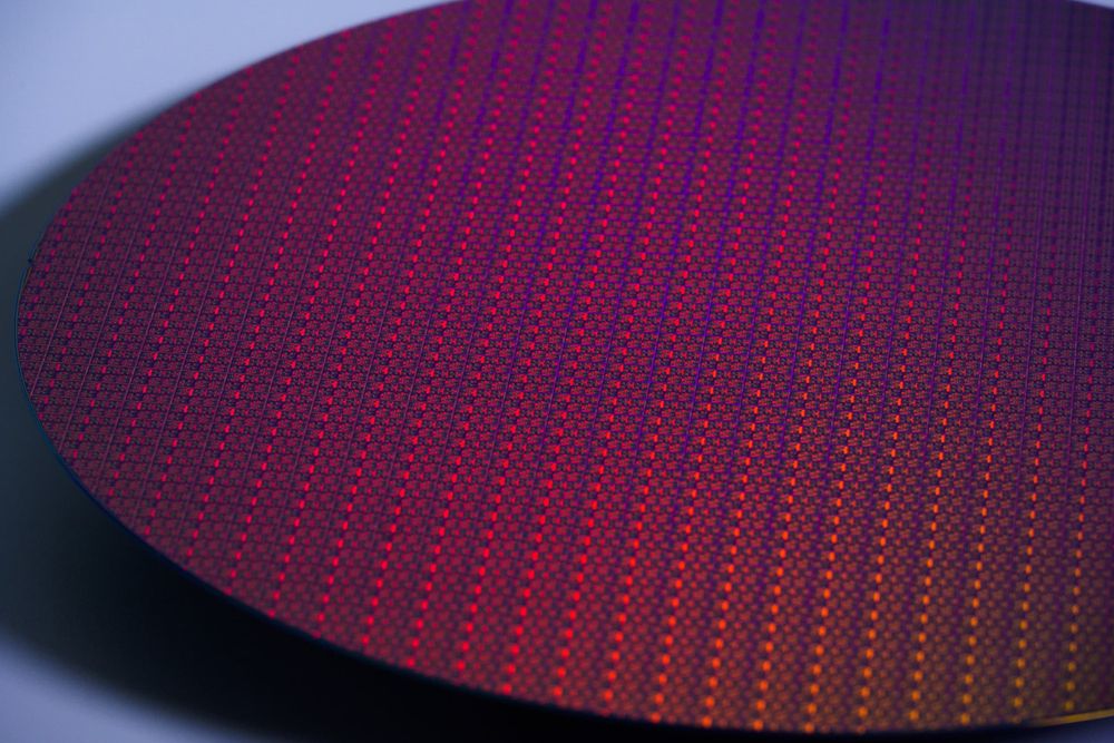
Numbers showing more than 18% power reduction and more than 9% performance improvement are pushing Intel Foundry back into the center of the leading-edge process race. Intel 18A-P, unveiled at VLSI 2026, is a refined version of 18A built on the foundation of RibbonFET and PowerVia. Meanwhile, TSMC N2 surpasses Intel 18A in transistor density, holding the lead in advanced manufacturing. On top of this, reports of Apple evaluating an entry-level M-series chip and Google considering advanced packaging are converging, and the axis of competition is beginning to expand from "the finest process" to "sufficient efficiency and supply diversification."
18A-P advances power, performance, and design libraries simultaneously
Intel 18A-P, unveiled at VLSI 2026, runs at more than 18% lower power for the same performance, or delivers more than 9% higher performance at the same power. According to Intel's explanation, this improvement comes from the co-optimization of transistor performance, wiring, and design technology. 18A-P is a refined version of 18A, inheriting the two core technologies of RibbonFET and PowerVia. For Intel Foundry, these figures represent the first strong material it can present to external customers.
Supporting both high-density and high-performance libraries gives chip designers a choice between area and speed. High-density libraries pack more circuits into the same area, while high-performance libraries suit designs that prioritize frequency or response speed.
The addition of threshold voltage (VT) pairs provides finer-grained control over the use of cells aimed at suppressing leakage current versus cells aimed at high-speed operation. A 30% improvement in skew corners over 18A is another factor that widens the design margin against manufacturing variation.
RibbonFET and PowerVia separate the congestion of current and signals
RibbonFET is a Gate-All-Around (GAA) type transistor, in which the gate surrounds the channel from all four sides. Conventional Fin Field-Effect Transistors (FinFETs) controlled multiple surfaces of a three-dimensional fin with the gate. In GAA, the gate wraps around the thin ribbon through which current flows, making it easier to more strictly control the on/off switching. As leakage current tends to increase in more miniaturized generations, this controllability has a greater impact on power efficiency.
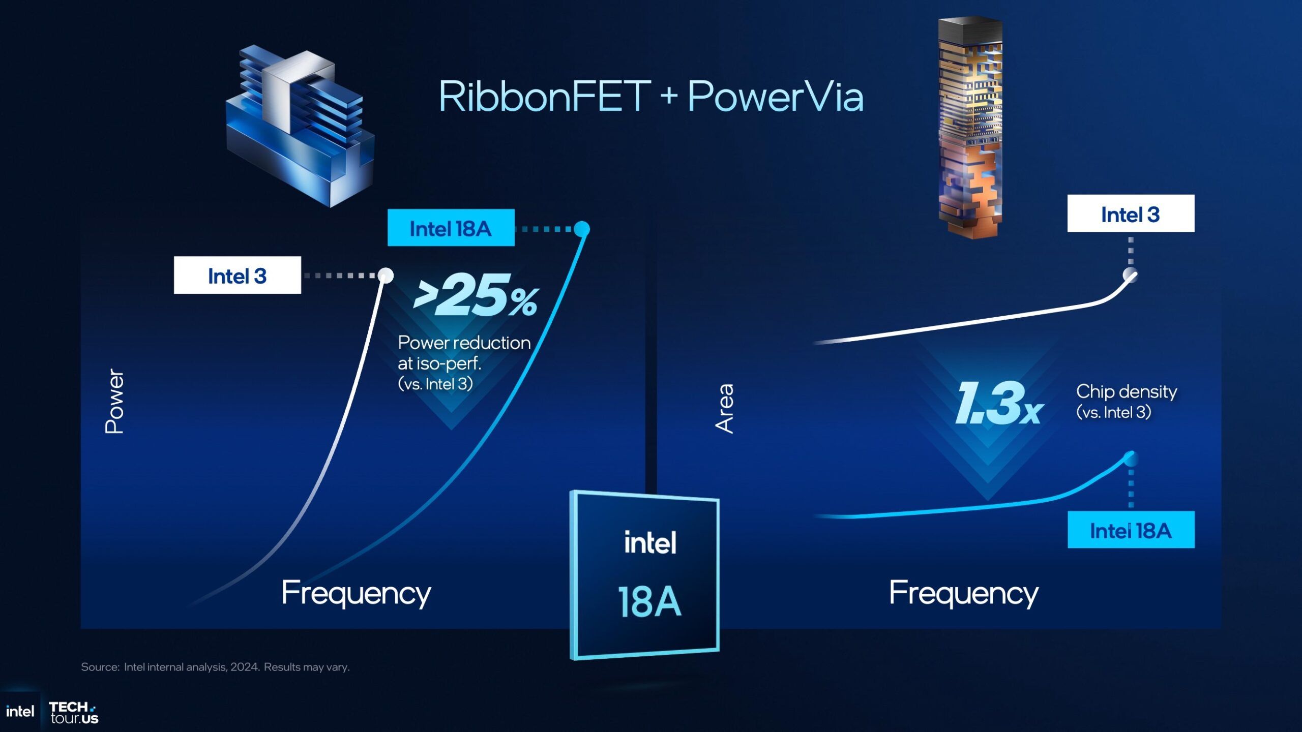
PowerVia is a backside power delivery technology that moves the wiring supplying power to the back of the wafer. In conventional chips, signal wiring and power wiring compete for the same front-side layers, and wiring resistance and congestion limited performance. By routing power wiring to the backside, the front side becomes easier to use for signal wiring, and voltage drop is also easier to suppress. The accumulation of these two technologies forms the foundation for the figures shown by 18A-P: "more than 18% lower power, more than 9% higher performance."
A divergence between TSMC N2's density and Intel 18A-P's efficiency
According to disclosed information, TSMC N2's transistor density is 313MTr/mm², while Intel 18A's is 238MTr/mm². Looking at density alone, TSMC N2 exceeds Intel 18A. On the other hand, the Intel 18A family shows more than a 30% density improvement over Intel 3, and 18A-P emphasizes gains in power and performance. Competition in leading-edge nodes needs to be viewed by separating area, power, speed, and supply capability. Comparing the key metrics yields the following:
| Item | Intel 18A / 18A-P | TSMC N2 |
|---|---|---|
| Transistor density | 238MTr/mm² (18A) | 313MTr/mm² |
| Power efficiency | 18A-P: more than 18% lower power at same performance | 24-35% lower power vs. N3E |
| Performance | 18A-P: more than 9% improvement at same power | 14-15% improvement vs. N3E |
| Structure | RibbonFET, PowerVia | GAA generation |
| Positioning | Emphasizes efficiency and backside power delivery | Emphasizes density and mass-production track record |
TSMC N2 claims a 24-35% reduction in power consumption, a 14-15% improvement in performance, and a 1.15x density improvement compared to N3E. Intel 18A-P's figure of more than 18% lower power should be read not as a direct comparison with TSMC N2, but as an improvement within Intel's own 18A family. Given the gap in density, Intel is not positioned to win head-on in terms of transistor count per unit area. The significance of 18A-P lies in whether the density gap can be compensated for through efficiency, design flexibility, and combination with advanced packaging.
Reports of Apple and Google evaluations signal supply diversification
It was previously reported that Apple is evaluating Intel 18A-P for an entry-level version of its M-series chips. The chips cited as targets are M-series chips for the MacBook Air and iPad Pro. There is speculation that production timing could be around Q2 to Q3 of 2027. However, no official statement has been issued by Apple regarding this, and at this stage it should be treated as a report of an evaluation phase rather than an adoption decision.
In addition, it has also been reported that Google is considering Intel's Embedded Multi-die Interconnect Bridge (EMIB) for its next-generation Tensor Processing Unit (TPU). EMIB is Intel's advanced packaging technology for connecting multiple semiconductor dies at high density on a substrate. Reports have used the notations TPUv8e and TPUv9 inconsistently, so the generation name cannot be treated as confirmed information. What matters is that Google's interest extends not just to the manufacturing process alone, but also to the packaging technology used to assemble AI accelerators.
The wall of mass-production proof that the loss-making Intel Foundry must clear
Intel Foundry posted an operating loss of $2.4 billion in Q1 2026, an improvement of $72 million from the previous quarter. The scale of the loss remains large, and unless external customer mass-production projects are accumulated, the outlook for the business will not change. Intel states that it is in discussions with multiple customers as of 2026, and that early wafers of 18A-P are already in the fab. As the company moves from technology announcements to mass-production track record, yield, delivery times, and the completeness of design support will be put to the test.
CEO Lip-Bu Tan stated that with the expansion of inference-oriented artificial intelligence (AI) and agentic AI, the ratio of central processing units (CPUs) to graphics processing units (GPUs) is shifting from the conventional 1:8 toward 1:1. If this view is correct, demand for server CPUs will strengthen again, expanding the room for Intel's design assets and manufacturing assets to come together. AI-era semiconductor demand tends to be seen as GPU-centric, but inference processing, data preparation, and control processing also require CPU capability. For Intel Foundry, 18A-P could also serve as an entry point for capturing peripheral demand from AI infrastructure.
The success or failure of 18A-P will not be determined by whether it exceeds TSMC N2 in density. What the reports of evaluations by Apple and Google indicate is a move by major tech companies to diversify their sourcing of leading-edge nodes and packaging options. If Intel Foundry can turn this opportunity into a mass-production track record, the advanced semiconductor market will move from TSMC's sole dominance toward a competition in which manufacturing and packaging partners are chosen based on the best fit for each application.