


On August 24, 2026, Intel disclosed the architecture of its next-generation Xeon processor, codenamed "Diamond Rapids," at Hot Chips 2026. The chip will support up to 256 cores and 1.28GB of last-level cache (LLC), with 16 memory channels reaching up to 12,800MT/s using MRDIMMs. That's double the physical core count of Intel's current top-tier P-core Xeon. But the more significant design shift isn't the core count itself—it's how Intel plans to move data to all 256 cores without creating bottlenecks.
Intel's answer is a new SoC layout called the "Fan-out Fabric." Sixteen core chiplets are grouped into four compute blocks, while memory controllers and I/O are consolidated into two separate fabric hubs. The reasoning behind rearranging how cores, cache, and memory connect is to let core count and data-supply capacity scale independently of each other.
Rewiring the Data Path With 16 Chiplets and Two Hubs
The top-end Diamond Rapids configuration packs in sixteen 16-core chiplets. Four chiplets stack onto a single base tile, and four such groupings combine—16 cores × 4 chiplets × 4 groups—to reach 256 cores. The core chiplets are built on Intel 18A-P, while the base tiles use Intel 3-T. Two additional fabric hubs, manufactured on Intel 3, house the memory and I/O subsystems.
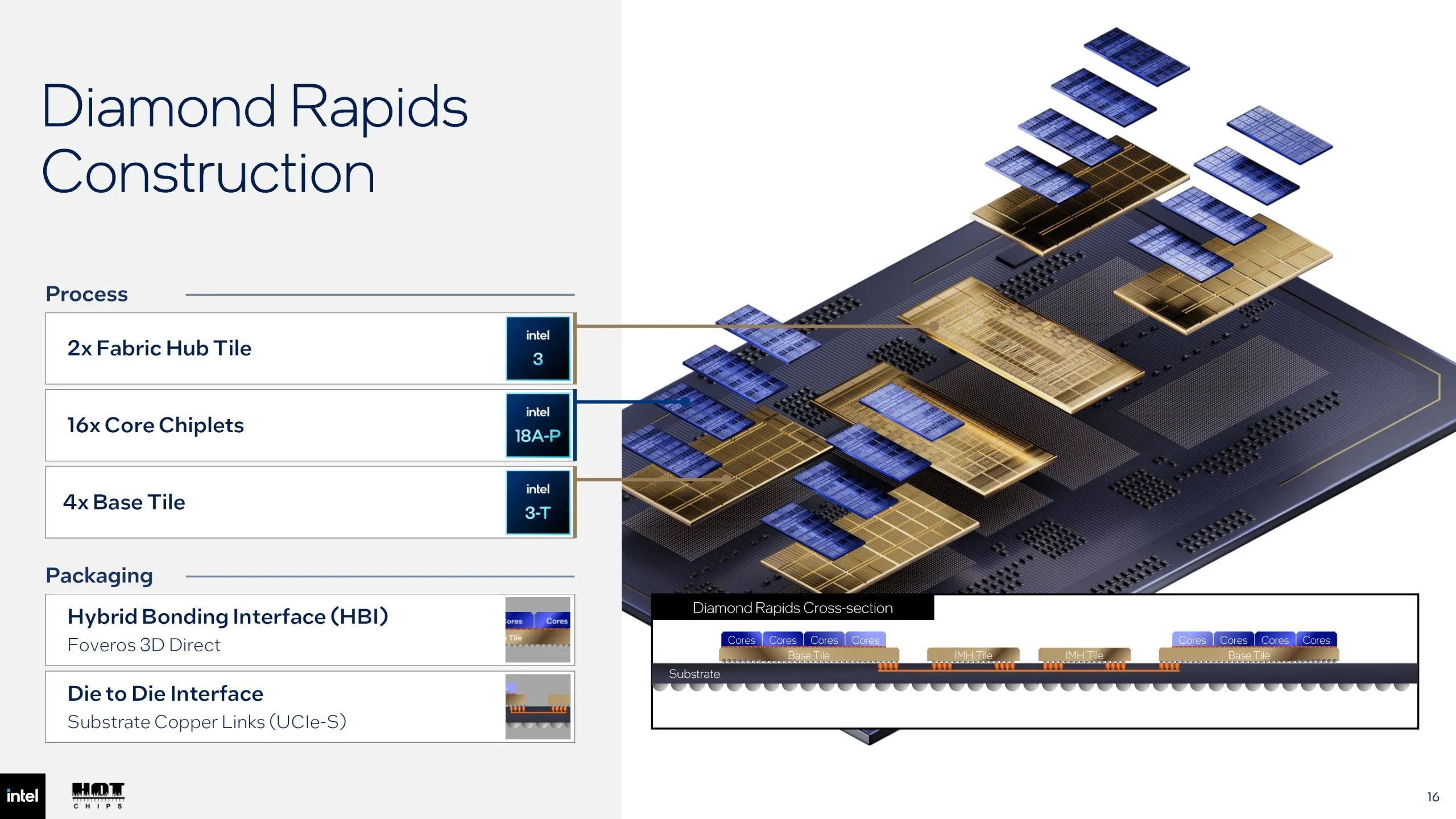
Chiplets connect to their base tiles using Foveros Direct 3D, a copper-to-copper hybrid bonding technique. Each core carries its own dedicated L2 cache, while the four chiplets on a given base tile share that tile's LLC. Each of the four base tiles holds 320MB of LLC, for a combined total of 1,280MB.
The fabric hubs link to the four compute blocks via UCIe-S, an industry-standard interconnect that runs through substrate wiring rather than a silicon bridge. Notably, none of the four compute blocks is locked to a single hub—each connects to both. According to on-site commentary reported by Tom's Hardware, Intel chose UCIe-S over EMIB specifically because it could create low-latency, uniform paths to every memory hub.
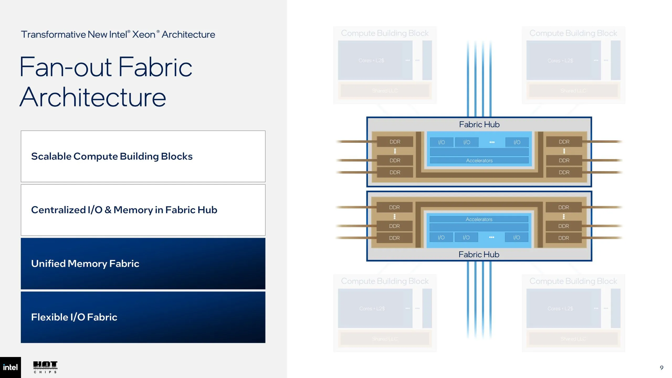
That "uniform" language describes a design goal, not a measured result. Dual-hub connectivity doesn't simply double available bandwidth, nor does it eliminate latency differences between compute blocks. Still, by avoiding a fixed pairing between any compute block and a single memory hub, Intel can reduce routing imbalances when distributing data across 256 cores. The core idea behind the Fan-out Fabric is separating the scaling of core count from the scaling of memory and I/O connectivity.
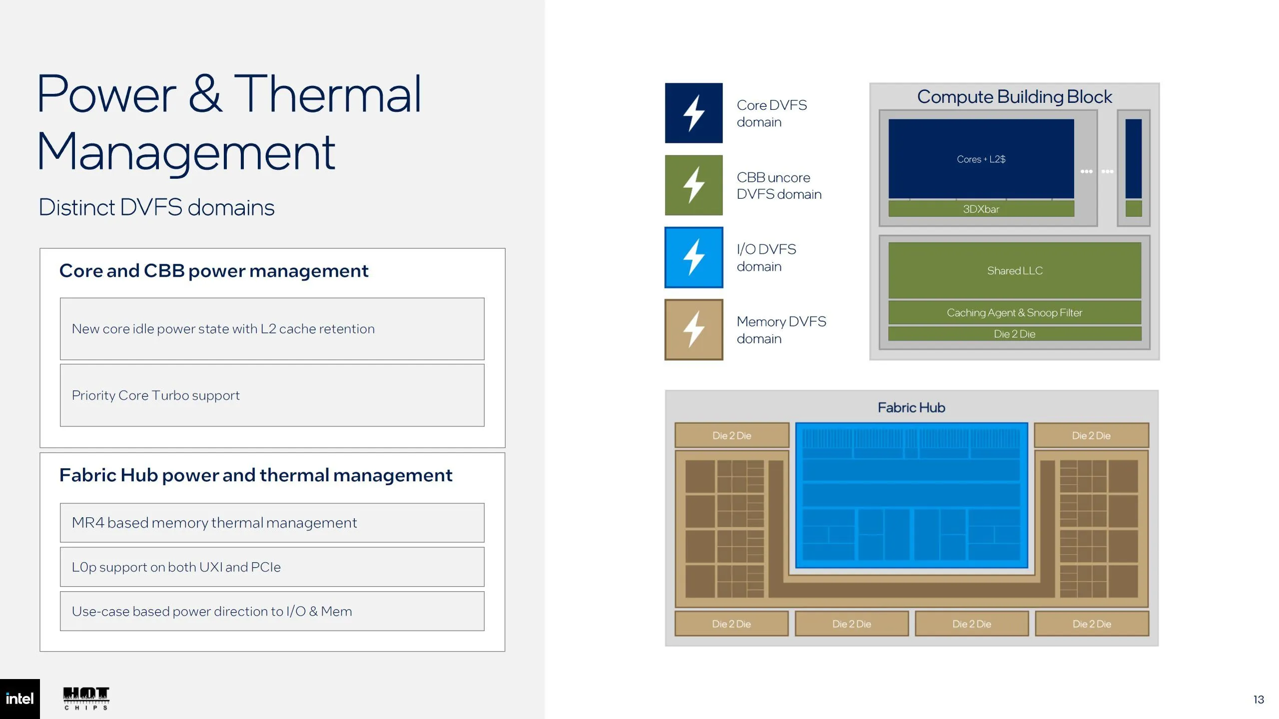
Power management has also become more granular to match this modular structure. According to Hot Chips presentation slides, cores, CBB uncore, I/O, and memory each have independent DVFS domains. On the core side, Intel introduced a new idle power state that retains L2 cache along with Priority Core Turbo; on the hub side, it added MR4-based memory thermal management and UXI/PCIe L0p states. The design allows power to be shifted between I/O and memory depending on workload, but Intel hasn't yet disclosed improvements to TDP or performance-per-watt.
In the current Granite Rapids design, a single compute die houses cores, part of the cache, and the memory controller together. Diamond Rapids breaks that arrangement apart, treating the compute side and the data-supply side as separate components. However, Intel has not disclosed measured latency across compute blocks, nor has it revealed manufacturing yield figures. Details of the core microarchitecture were also absent from this disclosure, so it remains too early to judge how the 16-way subdivision will affect real-world performance or product cost.
Dividing by Core Count Erases the Bandwidth Gain
Memory support includes 16 channels of DDR5-8000, with MRDIMMs pushing transfer rates up to 12,800MT/s. Assuming 64-bit channels, the theoretical bandwidth works out to 16 × 8 bytes × 12.8GT/s = 1,638.4GB/s—consistent with Intel's stated figure of roughly 1.6TB/s. By comparison, the current Xeon 6980P uses 12 channels with MRDIMM-8800, yielding 844.8GB/s under the same calculation. That puts the theoretical socket-level bandwidth increase at roughly 1.94x.
| Peak Specification | Diamond Rapids | Xeon 6980P (Granite Rapids) |
|---|---|---|
| Physical cores | 256 | 128 |
| LLC | 1,280MB | 504MB |
| Memory channels | 16 | 12 |
| MRDIMM transfer rate | 12,800MT/s | 8,800MT/s |
| Theoretical memory bandwidth | 1,638.4GB/s | 844.8GB/s |
| PCIe | Gen 6, 128 lanes | Gen 5, 96 lanes |
Dividing these figures by core count changes the picture. A simple calculation comparing the top-tier SKUs of each generation shows theoretical bandwidth per core slipping slightly, from 6.6GB/s to 6.4GB/s. That's because bandwidth grows by about 1.94x while core count doubles. This isn't a comparison of actual sustained bandwidth, but the theoretical per-core figure for the 256-core chip doesn't exceed that of the current 128-core SKU.
LLC tells a different story. Dividing the stated 1,280MB by 256 cores yields 5MB per core, about 27% more than the 3.94MB per core on the 6980P (504MB ÷ 128 cores). That comparison is only valid at the level of published specifications. A larger cache can reduce trips to external memory if workload data fits within it, but actual cache hit rates depend heavily on the workload itself—and Intel has not yet published measured results.
Matching AMD's 256-Core Milestone—Where the Real Differences Lie
AMD has also announced 256 cores and 16 channels of DDR5 for its sixth-generation EPYC 9006 "Venice" processors. Its MRDIMMs likewise reach up to 12,800MT/s, I/O uses PCIe 6.0, and memory bandwidth also comes in around 1.6TB/s. AMD is manufacturing Venice on TSMC's 2nm process. On paper, the headline core count and memory specs of the two chips are now roughly matched.
However, AMD has explicitly stated that its 256 cores support up to 512 threads. Intel has not disclosed a thread count for Diamond Rapids in this official summary, so there's no confirmed figure to directly compare against AMD's number yet.
Equal core counts don't guarantee equal server throughput. Per-core performance, simultaneous thread capacity, memory latency, and power constraints all differ between designs. Intel's move to 256 cores brings it level with AMD on headline specs, but the real competition will be decided by how much work each chip can complete within the same power envelope and price.
How Far Can APX and 18A-P Push Real-World Performance?
Diamond Rapids also brings major updates to the x86 instruction set. Advanced Performance Extensions (APX) expand general-purpose registers from 16 to 32, letting compilers keep values in registers for longer stretches of code. In Intel's prototype simulations, recompiling SPEC CPU 2017 integer benchmarks with APX support reduced load instructions by 10% and cut store instructions by more than 20%. These are simulation results, not measurements from physical hardware.
APX isn't a feature that automatically benefits existing binaries. Intel doesn't expect developers to rewrite source code, but realizing the gains requires recompiling with an APX-aware compiler. Dynamic languages will only benefit once their runtimes add support as well—meaning that even though the instruction set is built into the silicon, real-world adoption will depend on how quickly software catches up.
AVX10.2 and an enhanced version of AMX, both arriving alongside APX, target different workloads entirely. While APX broadly supports general integer code, AVX10.2 focuses on vector processing and AMX on matrix operations. Lumping these features together under a generic "CPU performance boost" label risks misunderstanding their actual scope. The real-world payoff depends on whether compilers, runtimes, and numerical libraries actually put the new instructions to use.
Manufacturing relies on Intel 18A-P. Intel evaluated a fully routed block based on a standard Arm core sub-block at 0.75V, claiming more than 9% higher performance at the same power, or more than 18% lower power at the same performance, compared to 18A. A separate thermal characterization study reported a 20-40% reduction in overall stack thermal resistivity when combined with certain design techniques. Neither figure means Diamond Rapids itself will run 9% faster than Granite Rapids. Since the base tiles and fabric hubs use Intel 3-family processes, the package's overall power draw and heat output will need to be measured in actual silicon.
Many numbers remain unpublished. Per-SKU clock speeds and TDP, pricing, and shipping dates—the details buyers actually need—are all still missing. Beyond that, sustained application bandwidth relative to the theoretical 1.6TB/s ceiling, and latency across the four compute blocks, still need verification. Diamond Rapids' redesign will have proven successful not simply because it packs in 256 cores, but because it can keep those 256 cores fed with data—without stalling, and within an acceptable power budget.