

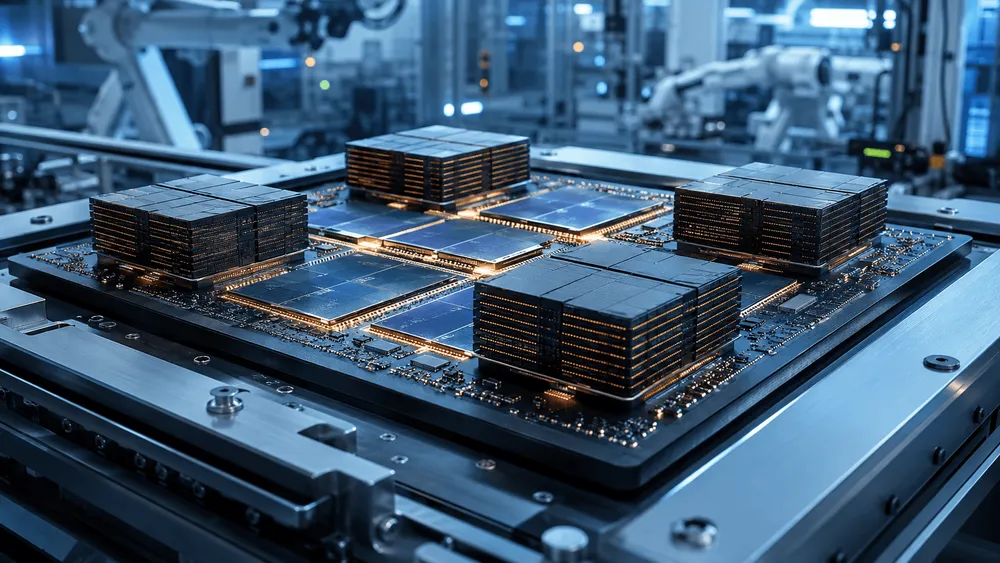
Intel is moving its next-generation advanced packaging technology, "EMIB-T," toward customer volume production in 2027. In its Q2 2026 earnings call on July 23, the company explained that its backlog is growing and that yield and reliability have reached target levels. On July 31, major substrate maker Unimicron also told DIGITIMES that full-scale volume production would come in 2027.
Driving this momentum is TSMC's supply constraints. On July 16, TSMC CEO C.C. Wei acknowledged that his company's advanced packaging capacity is so tight it is limiting customer growth, and he welcomed alternatives like EMIB-T. The center of competition has shifted from records for maximum package size to who can actually supply usable volume at a workable price.
The Clock Moves Toward 2027 Customer Volume Production
Intel described customer interest in EMIB-T as "very high," noting that its backlog continues to grow. The company said yield and reliability have reached internal targets, and it is now entering a phase of scaling up volume while maintaining high quality to support customer launches in 2027. This marks a shift from the stage of gathering customer evaluations to preparing for increased production in 2027.
Six months earlier, the situation was somewhat more ambiguous. At a briefing on February 25, Unimicron's Marketing Director Chu-Hua Yang said that major customers wanting to avoid CoWoS supply wait times were evaluating EMIB, but did not indicate a timeline for volume production. With this latest 2027 outlook, the projected timing for volume production has become more concrete than before. However, neither Intel nor Unimicron has disclosed customer names, product names, or planned quantities.
On June 18, Intel restructured its advanced packaging operations into a business led by a dedicated leader, appointing former SK hynix CEO Seok-Hee Lee to head it. This organization handles everything from technology development to back-end manufacturing under one roof, moving EMIB-T and HBI toward full-scale volume production for customers. The 2027 date is a roadmap target, not a record of shipped volume production units. Still, the organization, backlog, and supply plans are now beginning to point toward the same timeframe.
Conventional EMIB has been in volume production since 2017, combining Intel-made and externally made dies. However, EMIB-T is not a product name that can simply carry over the same track record. It adds through-silicon vias (TSVs) to a small bridge, adopting a structure that delivers power vertically near the HBM. Changing the power delivery path requires re-examining everything from substrate design to assembly and reliability testing. What Intel is aiming to launch in 2027 is volume production of this TSV-equipped generation for external customers.
On the technical side, test results supporting the move to volume production are beginning to accumulate. At ECTC 2026, Intel demonstrated a package exceeding 120×120mm that housed over 9x reticle-equivalent compute and memory silicon, achieving signal transmission of over 12Gbps with HBM4E and 64Gbps with UCIe. The achievement of shrinking connection pitch to 25µm came from a separate test vehicle. While these results provide grounds for designing large-scale products, they are not proof of high-yield volume production of finished products meeting the same specifications.
90% vs. 60% Is Not a Discount Rate
The cost difference in EMIB-T stems from a structure that doesn't cover the entire area with silicon. In full-area interposer approaches like CoWoS-S, a large wiring surface is created beneath both the compute die and HBM. EMIB-T instead embeds a small silicon bridge only at the boundary where adjacent dies connect at high density. Fine connection pitches are needed only around the bridge, while the center of the die can maintain wider spacing. It's a design that concentrates spending on wiring density only where needed.
According to Intel's estimates, the utilization rate of wafers used to make the small bridges is about 90%. In contrast, a full-area interposer covering more than 8x reticle-equivalent area can see utilization drop to around 60%, since a large rectangular shape must be cut from a circular wafer. Depending on conditions, the gap can reach as much as roughly 30 percentage points. Using less silicon is EMIB-T's key advantage.
However, 90% versus 60% is a comparison of material utilization rates, not a discount rate on finished packages. While Intel states that overall EMIB assembly yield is comparable to FCBGA of similar complexity, it has not disclosed the actual yield for volume-produced ultra-large EMIB-T packages made for external customers. If substrates become more expensive or defects increase during assembly and inspection, the savings gained from the bridge shrink. Intel also has not disclosed what percentage cheaper the finished package is compared to CoWoS.
Care is also needed when comparing to alternatives. While TSMC's CoWoS-S uses a silicon interposer, CoWoS-R adopts an RDL interposer made of copper wiring and resin, and has been in volume production since 2023. CoWoS-L embeds local silicon interconnects into a molded interposer using RDL, with the 3.5x reticle version entering volume production in 2024. The material cost gap Intel presents relative to full-area interposers cannot be applied uniformly across all CoWoS variants.
Why TSMC Welcomes Alternative Capacity
TSMC is not dismissing EMIB-T as a threat. In the Q2 2026 earnings call, CEO C.C. Wei said that because insufficient advanced packaging capacity is holding back customer growth, the company welcomes competitors that add flexibility to the market. If compute dies manufactured by TSMC can be integrated into packages by companies like Intel, TSMC's front-end revenue can still grow. Winning in wafer fabrication and winning in back-end packaging are not the same contest.
TSMC also has its own large-scale expansion plans. As of 2026, it is producing 5.5x reticle CoWoS, and in 2027 it plans to mass-produce a 9.5x version integrating 12 or more HBM units. By 2028, the roadmap calls for a 14x version carrying approximately 10 large compute dies and 20 HBM units.
Meanwhile, Intel plans to expand to over 8x reticle, approximately 6,800mm², in 2026, and to over 12x reticle, approximately 10,000mm², by 2028. The latter envisions 16 or more HBM4 or HBM5 units along with 30 or more EMIB-T bridges. In terms of sheer maximum area alone, TSMC's 2028 plan is larger. What Intel is pursuing is a different production pathway—one that reduces material usage through localized bridges while combining heterogeneous dies, including those made by TSMC.
Three Numbers That Will Prove Volume Production
The numbers to watch for in 2027 are the assembly yield of customer products, monthly shipment volume, and contract pricing. Intel has stated that yield and reliability have reached target levels, but has not disclosed what those targets actually are. It also remains unclear whether the growing backlog consists of prototype allocations or long-term volume production contracts.
The supply chain faces the same test. In its Q2 2026 report, Intel explained that shortages continue not only in advanced wafers but also in memory and substrates, and that it is rushing to secure both. Even if EMIB-T avoids CoWoS wait times, finished product volume won't increase if HBM or high-performance substrates remain scarce.
If Intel ships volume-produced products with named customers in 2027 and can lower contract prices without sacrificing yield, EMIB-T will become a practical second production pathway to fill the gap left by CoWoS shortages. Until that point is reached, the material utilization advantage and actual volume production competitiveness need to be evaluated separately.