

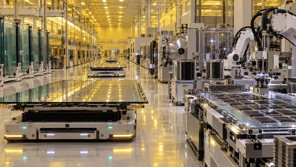
A fierce contest among leading semiconductor and AI infrastructure companies has emerged over the sale of Japan Display's (JDI) Mobara plant in Mobara City, Chiba Prefecture, where production has already been halted. According to Korea's ZDNet, U.S. memory giant Micron Technology and several data center operators have submitted letters of intent (LOIs) to JDI, while Korean semiconductor package substrate makers have also joined the acquisition talks. The sale price under discussion is reportedly approaching 500 billion won (roughly ¥55 billion). JDI itself confirmed in its August 2026 earnings announcement that it is continuing discussions with multiple candidates regarding the sale of the Mobara plant's assets.
The Mobara plant was once JDI's flagship facility, mass-producing small and medium-sized LCD panels as well as Generation 6 (G6) OLED panels for products such as the Apple Watch. However, facing intense competition in the panel market and a heavy fixed-cost burden, JDI ended panel production at the plant in November 2025. With domestic production consolidated at its Ishikawa plant, Mobara's vast clean rooms and power supply infrastructure were left as idle assets on the market.
At first glance, it may seem strange that a decommissioned display plant is now attracting intense interest from the front lines of semiconductors and AI infrastructure. The reason lies in a shift in the bottleneck for cutting-edge semiconductors—from front-end miniaturization to back-end packaging—where the time required to build new facilities has itself become the single greatest constraint.
Why Mobara's "Time Advantage" Is So Valuable
The biggest reason semiconductor makers and data center operators are eyeing an existing display plant is the dramatic reduction in time-to-operation it offers. Building a new semiconductor fab or hyperscale data center from bare land requires years—covering site selection, environmental assessments, obtaining local government permits, and securing high-voltage power supply and industrial water access.
Amid rapidly growing demand for AI chips, a delay of even a few years can mean the loss of critical market opportunity. If a buyer acquires the Mobara plant, it can skip the entire building construction phase and simply refurbish existing clean rooms and piping systems before moving in equipment.
That said, not every use case can be adopted unconditionally. The equipment specifications at Mobara carry clear advantages and disadvantages depending on the intended application.
| Conversion Candidate | Suitability of Mobara Plant | Key Advantages | Remaining Technical/Operational Challenges |
|---|---|---|---|
| Semiconductor front-end (wafer processing) | Unsuitable | Reuse of existing building | Clean room cleanliness falls short of sub-10nm miniaturization standards |
| Advanced packaging and testing (back-end) | High | Matches clean room standards, load-bearing capacity, ceiling height | Conveyance systems need conversion to semiconductor specifications; substation equipment needs upgrading |
| Glass core substrate manufacturing | Very High | Proven handling of Gen 6 glass substrates (1500×1850mm); large-scale exposure and deposition know-how | Additional introduction of ultra-fine wiring processes for package substrates |
| AI data center | High | Large site area, water-cooling capability via industrial water supply, location near the greater Tokyo metropolitan area | Major expansion of high-voltage power supply for server room conversion; floor load reinforcement |
As the table shows, the Mobara plant is not well suited to front-end fabs that form microscopic circuits on silicon wafers. However, it has a fundamental structure extremely well matched to back-end processes that cut, stack, and seal wafers, next-generation packaging lines using glass substrates, and data centers housing large fleets of AI servers.
Hiroshima's ¥1.5 Trillion Investment and the Domestic Back-End Gap
The leading candidate among prospective buyers, Micron, is aiming to build out a domestic back-end supply chain in Japan. As reported by Nikkei in March 2026, Micron is expanding advanced DRAM production capacity at its Hiroshima plant, investing approximately ¥1.5 trillion to build a new facility equipped with extreme ultraviolet (EUV) lithography equipment. The new building is expected to begin mass production of cutting-edge DRAM at the so-called "1-gamma" node around 2028.
The advanced wafers produced at the Hiroshima plant are processed into high bandwidth memory (HBM) and high-performance DRAM essential for AI servers. However, expanding front-end wafer fabrication alone does not complete the product. Advanced packaging processes—precisely placing stacked DRAM dies on silicon interposers, resin sealing, and fine bump connections—along with rigorous testing, are indispensable.
Micron has traditionally relied heavily on facilities in Taiwan and Southeast Asia for much of its back-end work. But given rising geopolitical risk, increasing transportation costs, and the need to align with support measures from Japan's Ministry of Economy, Trade and Industry, securing a robust domestic back-end base near Hiroshima's front-end operations has become an urgent priority.
If Micron acquires the Mobara plant, it could avoid years of civil engineering work and align a domestic assembly and testing hub with the 2028 launch of the new Hiroshima building. According to Nikkei, Micron initially aimed to reach an agreement by June 2026, but negotiations continue as details around power infrastructure upgrades and the scale of back-office renovations are still being scrutinized.
Suitability for Glass Substrates and Data Centers
Alongside Micron, the entry of Korean semiconductor package substrate makers has also drawn attention. The semiconductor industry is currently in the midst of intensifying competition to shift from conventional organic resin package substrates to "glass core substrates," which offer superior flatness and heat resistance and can bring thermal expansion coefficients closer to that of silicon. Korean players such as Samsung Electronics, SKC subsidiary Absolics, and LG Innotek are racing toward commercialization.
The manufacturing process for glass substrates is far closer to that of liquid crystal display production lines than to silicon wafer fabrication. The Generation 6 glass substrates handled at the Mobara plant measured 1500mm × 1850mm, and the facility has accumulated technical expertise in transporting extra-large thin glass sheets without breakage and performing uniform exposure, deposition, and cleaning within large chambers. For semiconductor substrate makers, repurposing Mobara's buildings and clean room infrastructure would accelerate development and mass production far faster than building a large-scale glass processing plant from scratch.
Similarly, the Mobara plant holds strong appeal for data center operators. While data centers are already clustered in areas of Chiba Prefecture such as Inzai City, power allocation at existing sites is becoming tight. The Mobara plant, originally built with large-scale power receiving equipment and industrial water allocation for display production, would be relatively easy to retrofit with air conditioning and water-cooling piping. Precedents such as TSMC's acquisition of an Innolux plant in Taiwan for advanced packaging, and Sharp's transfer and leasing of its Sakai plant to SoftBank and KDDI for AI data center use in Japan, are bolstering the perceived value of the Mobara site.
Why Equipment—Not eLEAP Patents—Was the Prize
While negotiations over the sale of the Mobara plant itself continue, the fate of the manufacturing equipment installed there has already been settled. According to ZDNet, most of the manufacturing equipment related to "eLEAP," the next-generation OLED technology that JDI had been independently developing at Mobara, was purchased by China's display giant HKC.
eLEAP is a technology that directly patterns RGB subpixels using photolithography techniques similar to semiconductor manufacturing, rather than relying on fine metal masks (FMM) to deposit organic materials. It was expected to improve aperture ratio, boosting light emission efficiency and lifespan, but the Mobara plant never achieved stable yields for large panels, leaving the technology's mass-production viability only partially proven.
While the equipment was sold to a Chinese manufacturer, interest among buyers in JDI's core eLEAP patents themselves has been muted. JDI has already licensed the patent rights necessary for eLEAP's deposition equipment to companies such as U.S.-based Applied Materials. Even if a third party were to purchase the patents outright from JDI, it could not exclude rights already granted to companies like AMAT and use the technology exclusively.
Furthermore, competitors are independently advancing their own non-FMM OLED photolithography technologies—for instance, South Korea's LG Display unveiled a technology called "FLiPP" at the International Meeting on Information Display (IMID) in August 2026. With little incentive to pay a hefty price for patents that cannot confer exclusive rights, only the physical manufacturing equipment ultimately moved to the Chinese market.
A ¥55 Billion Deal at the Crossroads of JDI's Turnaround
Whether the Mobara plant sale negotiations conclude at around 500 billion won (roughly ¥55 billion) will be a decisive turning point for JDI's corporate turnaround.
JDI was formed under the leadership of the Innovation Network Corporation of Japan (now INCJ) by consolidating the LCD businesses of Sony, Toshiba, and Hitachi. For years, the company lagged behind the industry's shift to OLED for smartphones, accumulating losses along the way. After halting panel production at Mobara in November 2025, JDI transferred its Tottori plant and offered voluntary retirement packages as part of a restructuring effort aimed at cutting up to roughly ¥25 billion in annual fixed costs. As of the end of June 2026, the exercise of stock acquisition rights has progressed, securing ¥3.6 billion in net assets and narrowly resolving the company's negative net worth.
JDI is now restructuring its Ishikawa plant into a hybrid production hub for displays, sensors, and advanced semiconductor packaging, pursuing a "BEYOND DISPLAY" strategy centered on supplying bio-sample processing devices and backplanes for automotive HUDs. The interest shown by partner OLEDWorks in utilizing the Ishikawa plant's production line (backplane processes) rather than Mobara aligns with JDI's policy of concentrating production functions at Ishikawa.
If the sale of the Mobara plant secures roughly ¥55 billion in cash, JDI could strengthen its financial foundation and redirect funds toward new business investments at Ishikawa. However, closing the deal will require finalizing details such as cost-sharing for power infrastructure upgrades demanded by the buyer and setting deadlines for removing remaining infrastructure inside the buildings. Whether Mobara's clean rooms are reborn as a semiconductor back-end facility or transformed into a massive AI computing hub—the decision on the partner and terms, expected within a few months, will simultaneously shape the future of Japan's semiconductor supply chain and JDI's own survival.