

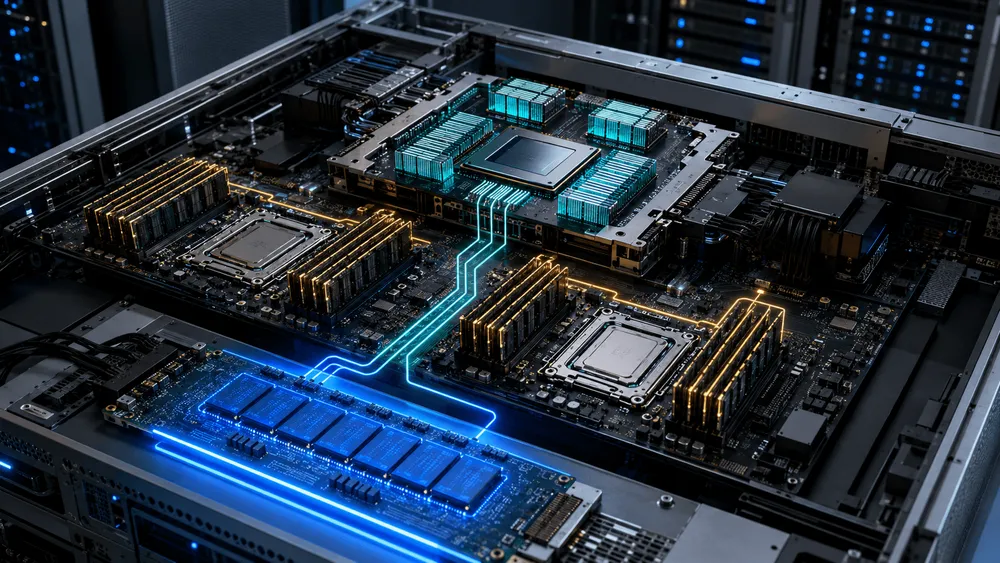
According to KIOXIA's announcement, the company will showcase its CXL-compatible memory expansion module, the "KIOXIA XL1 series," at FMS 2026, held in Santa Clara, California from August 4 to 6, and plans to ship evaluation samples to industry ecosystem partners in August 2026. What has been disclosed at this point is a plan for the exhibition and evaluation samples. It does not signify the start of mass production or general sales. What can be confirmed from KIOXIA's official FMS announcement is limited to the point that it will showcase a CXL memory module using XL-FLASH.
The goal is not to increase SSD capacity. The idea is to use the expensive, proximal DRAM and HBM in AI servers for frequently read "hot" data, while moving pages with lower access frequency to an external memory tier connected via CXL. XL1 is a module intended to place low-latency XL-FLASH into that outer tier.
In AI processing, the model body, KV Cache, and search indexes all similarly demand high-speed memory. However, it is not always possible to place all of them in a GPU's HBM or CPU-attached DRAM. This is because capacity, cost, and the number of available slots become constraints first. What XL1 aims for is not to replace the fastest memory, but to finely allocate which data uses the limited high-speed memory.
Flash entering the memory tier, not the storage tier
The list of FMS 2026 exhibits published by KIOXIA on August 3 includes the "CXL memory module using KIOXIA XL-FLASH." What was presented there was a direction of expanding the memory tier with XL-FLASH. The product name "XL1" and the explanation of placing infrequently accessed data on the module side are reported by TechPowerUp, which covered KIOXIA's announcement. What KIOXIA's official FMS announcement indicates is that it will showcase a CXL memory module using XL-FLASH.
KIOXIA describes XL-FLASH as a low-latency, high-performance flash designed to bridge the performance gap between DRAM and ordinary flash. It is non-volatile, and among the second-generation XL-FLASH, the products supporting the MLC feature are already in mass production. However, this is the general status of XL-FLASH as a medium, and does not mean that XL1 itself is in mass production.
This distinction matters greatly in practice. A typical SSD is placed outside of main memory, accessed via a file system or block I/O. CXL-attached memory expansion, on the other hand, is closer to the concept of increasing the number of tiers that the host treats as memory. Rather than increasing the places to store data, it creates tiers with different speeds within the memory space that the application requires. In AI servers, what is being tested is how much this use of separate tiers can alleviate the shortage of DRAM/HBM.
KIOXIA's investor materials from June 2025 stated a plan to sample "CXL attached XL-FLASH" in the second half of 2026. With this announcement to showcase it as the XL1 series at FMS 2026 and the indicated plan for evaluation samples in August, the plan to move the concept of using XL-FLASH for CXL-based memory expansion into evaluation samples has been shown. However, the CXL-XL configuration described in that material cannot be treated as the official specification of XL1.
Retaining hot data, moving infrequently accessed pages
CXL uses the PCIe physical layer while adding a mechanism for the host to access external memory. A general Type 3 memory expander, as defined in CXL 1.1, mainly responds to memory requests from the host via CXL.mem. Although it has not been announced that XL1 is Type 3, the basic behavior when considering CXL memory expansion follows this direction.
What matters here is access frequency rather than capacity itself. If data that a GPU repeatedly references, or an area that a CPU updates at short intervals, is pushed out to a distant tier, the latency directly translates into processing delays. Conversely, if it is a page that has not been read for a while—data that might be referenced later but does not need to be kept resident—moving it to the external memory tier can free up space in the high-speed memory.
Therefore, the value of XL1 cannot be measured by how many GB of DRAM/HBM it can replace. The OS, runtime, application, and server-side hardware need to cooperatively handle which data to move, when to bring it back, and ensuring processing is not delayed during the move. If it does not match the access pattern, data offloaded to external memory will be fetched repeatedly, and effective performance will not improve even if capacity is increased. If the management of the movement itself is heavy, even if free space is created in DRAM, it will consume the overall processing time.
In a design that increases the number of places to put pages, having free capacity and achieving usable performance are separate matters. If an area with concentrated access is moved to the external tier, latency accumulates. Conversely, if sufficiently cold data can be moved, the area necessary for continued processing can be preserved in HBM or DRAM. Where to draw that line changes depending on the model's configuration, batch size, and fluctuations in inference requests, so it cannot be determined solely from a module's spec sheet.
KV Cache offloading and memory tiering for AI inference are also being discussed as use cases for CXL at FMS 2026. However, the phrase "for AI workloads" merely represents the intended use case. How much XL1 will change training time or inference latency has not yet been disclosed. The same applies to throughput and GPU utilization.
Connecting via CXL does not mean it becomes as fast as DRAM
KIOXIA's past research offers material for considering how much latency in external memory can be tolerated. The company adjusted latency to a few microseconds using a CXL-compatible FPGA equipped with an Intel Agilex 7, and evaluated the graph processing algorithms BFS and SSSP. It reported that when the latency from the GPU to CXL memory was under approximately 2 microseconds, execution times were nearly equivalent to those of host DRAM.
However, this result cannot be read as the performance of XL1. The subject of evaluation was not actual XL1 hardware, nor was it AI training or inference. It was an initial verification of graph processing simulating latency with an FPGA, and the condition for success comes with the qualification of being "under approximately 2 microseconds." The read/write latency of XL1 has not been disclosed, and it cannot be estimated from this research result either.
What the research teaches us is that performance is not determined simply by adding a CXL-based tier. The tolerable latency changes depending on how randomly the application accesses data, how much the same page is reused, and how well memory management can grasp access frequency. If a new tier is placed between DRAM and external memory, both the speed of the medium and the mechanism of data placement must be measured.
Support for sharing or pooling remains unclear
CXL 2.0 added memory pooling using switches and features to provide capacity on demand. If configurations that share memory across multiple hosts are considered, a different design becomes possible compared to fixing and stacking DRAM per server.
However, it is not yet clear whether XL1 supports CXL 2.0, whether it can be used via a switch, or whether it can handle pools across multiple hosts. The CXL generation, number of PCIe lanes, and form factor are also unpublished. The features that the standard possesses and the features that an individual module implements need to be considered separately.
For the same reason, the hardware, OS, and memory tiering software compatible with XL1 are also unknown at this point. Even if the host can recognize external memory, unless it is determined which workload gets allocated how, the goal of moving infrequently accessed data outward cannot be put into operation. In the evaluation samples, in addition to hardware connectivity, it will be necessary to verify whether this kind of data differentiation is viable in real workloads.
What can only be compared once evaluation samples arrive
XL1's specific capacity, effective bandwidth, and read/write latency have not been disclosed. Power consumption and durability, as well as price and mass production timing, are also unknown. There are no performance figures for real AI applications either. Furthermore, the shipping schedule for August 2026 is for partner evaluation samples, and it has been indicated that some features are unverified and specifications may change.
Upon adoption, it will also be compared against adding more DRAM/HBM, offloading to TLC SSDs, and compressing or splitting KV Cache and search data on the application side. In addition to capacity, one must compare which latency and operational burden one is willing to accept. Whether XL1 can be adopted will be determined by measuring, in addition to total memory capacity, how much latency and operational burden are involved in using it for real workloads.
The direction of bringing NAND closer to the memory tier, outside of the storage tier, has become visible with this announcement. If the evaluation samples reveal capacity, latency, supported environments, and placement effectiveness in AI processing, it will become possible to judge which jobs the tier placed outside DRAM/HBM can actually take on.