

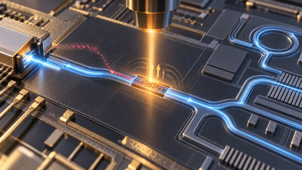
The semiconductor laser at the heart of optical communications is a surprisingly delicate device. Even a tiny amount of reflected light returning to the laser cavity from a fiber end-face or a circuit junction can cause the oscillation wavelength to drift and phase noise to spike, disrupting communication. The component essential for blocking this reflected light is the optical isolator. It allows light to pass in the forward direction while canceling out light traveling back in the reverse direction.
For years, however, the optical isolator has stood as the "final frontier" of silicon photonics integrated circuits. Achieving the non-reciprocal optical behavior needed—where light behaves differently depending on direction—requires a magneto-optical material such as cerium-substituted yttrium iron garnet (Ce:YIG). This material does not crystallize, and therefore exhibits no magneto-optical effect, unless it undergoes high-temperature annealing above 600°C after deposition. Heating an entire chip in a furnace would melt the metal electrodes already integrated on it and thermally damage the silicon waveguides. Because of this thermal incompatibility, optical isolators have long depended on hybrid assembly, in which a separately fabricated component is bonded onto the chip.
A research team led by Associate Professor Taichi Goto at Kyocera Corporation and Tohoku University's Research Institute of Electrical Communication has developed a method to overcome this thermal barrier using localized laser annealing. The team built a monolithic integration prototype in which a magneto-optical material is deposited on a silicon photonic circuit and then crystallized through localized laser irradiation, protecting the rest of the circuit from thermal exposure. The findings were published in the IEEE's peer-reviewed journal IEEE Access in September 2026 (DOI: 10.1109/ACCESS.2026.3729586).
The Faraday rotation value derived in this study reached approximately nine times that of previously reported laser-annealed Ce:YIG, demonstrating a level comparable to conventional separately fabricated devices—but achieved directly on a silicon photonic circuit.
The Logic of Localized Heat Treatment: Avoiding "Mass Execution" by Furnace Heating
Technology for integrating passive components and modulators onto silicon photonic circuits has drawn attention amid the explosive growth in data traffic driven by the rapid expansion of generative AI. In co-packaged optics (CPO), where processors and photonic circuits are placed in close proximity within the same package, minimizing electrical wiring distance to reduce transmission loss and power consumption is becoming a standard design approach. Stably driving the semiconductor lasers integrated into such systems requires an on-chip optical isolator capable of blocking reflected light within the chip itself.
However, the thermal budget demanded by magneto-optical garnet crystals has proven extremely harsh. Ce:YIG remains amorphous immediately after room-temperature deposition, and achieving sufficient Faraday rotation requires annealing at temperatures around 600°C to 800°C. Meanwhile, the multilayer wiring metals used in CPO, such as aluminum and copper, deform and interdiffuse even at temperatures around 400°C, destroying the circuit's electrical continuity. The silicon waveguides themselves also suffer from increased optical scattering loss at high temperatures, as interface roughness with the silicon dioxide cladding layer worsens.
As long as furnace annealing—which heats the entire chip uniformly—is used, coexistence of optical isolators and metal wiring remains unattainable. The research team focused on laser annealing, which combines selective light absorption with spatial localization, to address this problem. Using a diode laser with a wavelength of approximately 915 nm, they designed a system that narrowly focuses the beam onto the tiny trench region where the optical isolator is formed, applying short-duration irradiation only to that area.
The same research group had already reported an optical isolator technology using nanocomposite garnet in the journal ACS Applied Optical Materials in June 2026 (DOI: 10.1021/acsaom.6c00176). The study now published in IEEE Access is distinct in that it establishes a new monolithic integration method—combining a microtrench structure with localized laser heating to directly crystallize a Ce:YIG thin film without using a seed layer.
Kyocera describes this achievement as the world's first technology to integrate an optical isolator onto a silicon photonic circuit using a laser annealing method. This claim is based on the company's own investigation as of July 2026, and has not been comprehensively verified by an independent third party. Nonetheless, it stands out as a notable attempt to resolve thermal incompatibility through localized laser processing.
Design: Trench-Localized Irradiation and an Asymmetric Mach-Zehnder Interferometer
The device used for demonstration is based on an asymmetric Mach-Zehnder interferometer (AMZI) structure fabricated using a commercial silicon-on-insulator (SOI) process. The silicon core waveguide has cross-sectional dimensions of 550 nm in width and 180 nm in height, shaped to satisfy single-mode conditions. Multimode interference (MMI) couplers with low wavelength dependence were used as the elements for splitting and combining light between the two arms. A physical path-length difference of 15 was deliberately introduced between the two arms of the interferometer.
On one arm of the interferometer, a microtrench was opened by dry-etching through the silicon dioxide upper cladding layer. Three trench lengths were fabricated across different devices: 50 , 100 , and 200 . A Ce:YIG thin film was deposited directly into this opening using radio-frequency ion beam sputtering, without a seed layer.
| Item | This study (locally laser-annealed AMZI) | Conventional furnace-annealed baseline / prior studies | Source and measurement conditions |
|---|---|---|---|
| Integration method | Monolithic local integration (within microtrench) | Whole-chip furnace heating, or separate component bonding | IEEE Access / Kyocera published materials |
| Heat treatment method | Localized irradiation with 915 nm diode laser | Uniform isothermal furnace annealing (approx. 600–800°C) | Vacuum level below 80 Pa, substrate temperature held at 750°C |
| Optical isolation ratio | 13.6 dB | Approx. 15–30 dB (separately fabricated bulk device baseline) | Wavelength 1540 nm, TM polarization, 25°C |
| Insertion loss | 20.4 dB | Approx. 1–3 dB (practical bulk device baseline) | Measured value for 100 trench device |
| Propagation loss | 9.5 dB | Several dB or less (depending on waveguide structure) | Measured evaluation of Ce:YIG waveguide in trench section |
| Converted Faraday rotation | 0.092°/ | 0.010°/ (prior laser-annealed Ce:YIG) | Derived from 4.5 nm peak shift and FSR |
| Irradiation spot size | 700 square beam | Full furnace heating (millimeter scale to entire wafer) | Trench region only heated through anti-reflective window |
During the laser annealing process, the chip was placed inside a vacuum chamber (evacuated to below 80 Pa), and the substrate temperature was held at 750°C. A semiconductor laser with a center wavelength of 915 ± 15 nm and a maximum output of 120 W was shaped by an optical system into a uniform square beam measuring 700 on each side, and selectively irradiated onto the trench region through an anti-reflection-coated window. By confining the irradiation area within the microscale trench, the cracking caused by thermal expansion mismatch in the thin film—a problem that had plagued conventional wide-area laser annealing over 1 mm square—was completely suppressed.
Optical characterization was carried out in an environment where the chip temperature was precisely controlled to 25°C using a Peltier element. A tunable semiconductor laser was used to sweep the communication wavelength band from 1520 nm to 1610 nm. The polarization was fixed to TM, the mode in which the magneto-optical effect appears most prominently. Light was coupled in and out using lensed fibers connected to the end faces.
A samarium-cobalt (SmCo) permanent magnet was used to drive the magneto-optical effect. An external magnetic field exceeding the saturation magnetic field of Ce:YIG was applied in-plane to the chip's waveguide surface. To acquire forward and reverse transmission spectra without introducing realignment errors from repeated fiber insertion and removal, the measurement procedure kept the chip and optical fiber positions completely fixed while reversing the polarity of the permanent magnet.
Measured Device Performance and Structural Evidence of Material Crystallization
For the device with a 100 trench length, an optical isolation ratio of 13.6 dB was obtained at a wavelength of 1540 nm. This 13.6 dB figure represents the confirmed difference between forward and reverse transmission intensities. In its published materials, Kyocera translates this attenuation level as suppressing reflected light traveling in the reverse direction to roughly one-twentieth (about a 95% reduction). However, the absolute optical power values for forward and reverse directions used for this comparison are not disclosed in the available published materials or the paper itself.
Meanwhile, the insertion loss for forward-transmitted light was a substantial 20.4 dB. Although absolute optical power values were not disclosed, this figure reflects a significant attenuation of signal strength as it passes through the waveguide. The propagation loss of the waveguide within the trench section alone was recorded at 9.5 dB. The paper's authors conducted a detailed breakdown of the loss sources, estimating that losses caused by step discontinuities and interface roughness arising from the trench fabrication process account for approximately 66% of the total. Absorption and scattering losses associated with loading the Ce:YIG material itself were estimated at approximately 27%, while losses attributable to the interferometer structure itself, including the MMI couplers forming the AMZI, were estimated at approximately 7%.
Regarding the Faraday rotation, the key quantitative indicator of the magneto-optical effect, this study derived a converted value from the shift width of the interference spectrum rather than through direct measurement. The peak shift observed in the transmission spectrum upon reversing the external magnetic field was 4.5 nm. Based on this shift and the free spectral range (FSR) of 44 nm for the asymmetric Mach-Zehnder interferometer without Ce:YIG loading, along with the 100 trench length, the calculated Faraday rotation reached 0.092°/.
This value far exceeds the 0.010°/ previously reported for laser-annealed Ce:YIG. It approaches the standard range of values reported for other deposition methods, including furnace heating (0.021 to 0.113°/)—a favorable figure achieved through localized heating on a silicon waveguide.
Transmission electron microscope (TEM) observation of the microstructure physically confirmed the crystallization of the Ce:YIG thin film induced by localized heating. The deposited Ce:YIG layer measured 195 nm in thickness, and lattice analysis confirmed the formation of the (420) garnet crystal plane. The measured lattice spacing was $d = 0.273$ nm, showing high consistency with the theoretical bulk crystal value of 0.278 nm. Compositional analysis by energy-dispersive X-ray spectroscopy (EDX) revealed that the atomic ratio of cerium, yttrium, iron, and oxygen satisfied the garnet ratio of approximately 1:2:5:(12−). However, precise quantification of the oxygen deficiency was not achieved.
Structural analysis near the interface revealed an altered region approximately 10 nm thick at the boundary with the silicon waveguide. This altered region included a naturally formed oxide film () of about 5 nm, and localized segregation of cerium near the interface was also observed.
Unresolved Challenges Blocking Integration into Practical Circuits
This study demonstrated, at the laboratory scale, the possibility of completing the thermally demanding crystallization of Ce:YIG directly on a silicon photonic circuit. However, a technical gap remains before these results can be directly translated into the manufacturing of commercial photonic-electronic integrated chips.
The biggest obstacle is the extremely large insertion loss of 20.4 dB measured in this study. Although the absolute optical power values for input and output were not disclosed in the published materials, a device that causes this level of attenuation on its own is difficult to tolerate in a practical communication circuit for an isolator alone. Rigorous separation of the loss mechanisms—optical scattering, interface mismatch, and absorption—along with demonstrated reduction strategies, will be the focus going forward. The paper's authors list several improvement directions, including smoothing the trench sidewalls through improved dry-etching selectivity, reducing overetching into the underlying silicon waveguide, and controlling the valence of ions through oxygen partial pressure control during annealing. However, these are mentioned only as future considerations, and loss reduction has not been experimentally demonstrated.
Fundamental challenges also remain in the mechanism for applying the magnetic field. In this experiment, the saturation magnetic field was supplied by mechanically positioning a bulk SmCo magnet externally near the device. However, incorporating a bulk magnet inside the package of a silicon photonic integrated circuit could undermine the very advantages that integrated circuits are meant to provide, such as miniaturization and higher integration density. Unless a technology is established to monolithically form a magnetic thin-film bias layer directly on the chip surface, the device cannot truly be called a self-driven, genuine on-chip optical isolator.
Data on manufacturing yield and reliability also remain entirely absent. The data presented represent static optical measurements from a single test chip, and no information is provided regarding the uniformity or reproducibility of annealing quality across a wafer surface. Materials needed to assess commercial viability—such as long-term thermal cycling tolerance required in data center environments, proximity limits to metal electrodes, and resistance to external magnetic noise—have not yet been established. Whether localized laser annealing becomes a viable option for optical isolator integration will depend on future process improvements that substantially reduce insertion loss, as well as the successful development of a thin-film bias mechanism.