

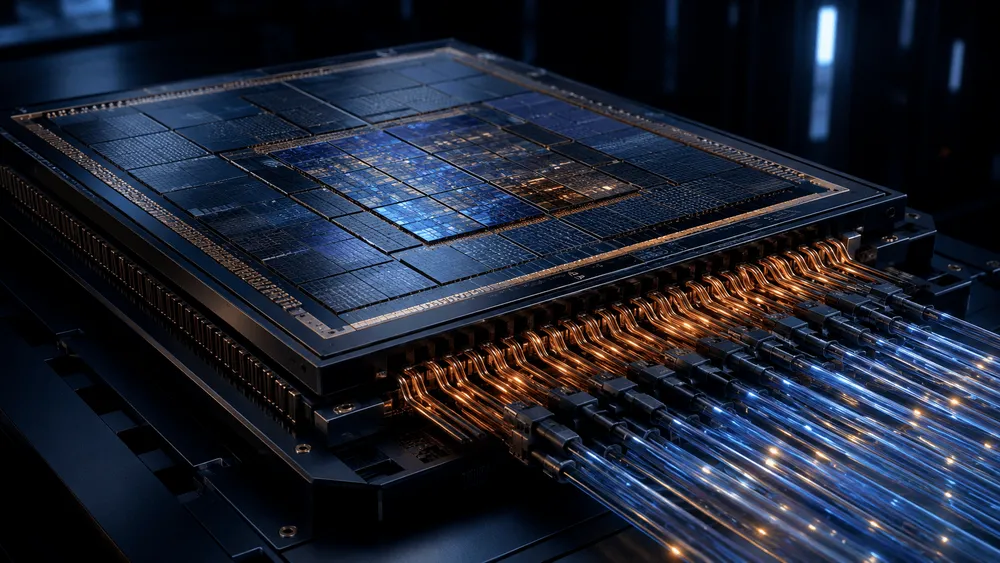
MediaTek is preparing a next-generation SerDes delivering roughly 400Gbps per lane for the second half of 2027. At the Q2 2026 earnings call on July 31, CEO Rick Tsai said development of the "400G or 448G" SerDes IP is progressing well, with readiness expected in the second half of 2027. Commercial Times reported that this technology is a foothold for competing over Google's TPU v10 and Meta's next-generation AI ASICs, but MediaTek has disclosed neither customer names nor design wins. What has been confirmed is not an order, but the timing of when the I/O technology needed to compete for the next design win will be in place.
448G Arrives in H2 2027, But No Customer Names Disclosed
MediaTek has officially laid out two AI ASIC roadmaps. The first AI accelerator, developed with a major US cloud provider, will begin mass production in Q4 2026. The second generation, which improves performance and total cost of ownership, targets mass production in early 2028, assuming packaging yield and reliability progress as planned. Data center revenue for 2026 is projected to exceed $2 billion.
The company estimates the 2027 SAM (Serviceable Addressable Market) for AI accelerators at $80 billion, and has raised its target share from 10–15% to 15–20%. This market size excludes CPUs, network switches, and HBM. For MediaTek, which has grown on the strength of smartphone SoCs, these numbers signal that data centers are beginning to become a new pillar of revenue.
However, the official transcript of the earnings call never mentions Google, Meta, or TPU. The customer is described only as "a major US cloud provider," and Tsai declined to answer when asked whether the company could become a primary supplier in the future. Commercial Times, citing supply chain sources, reported that MediaTek—using 336G SerDes—won a major order for Google's TPU v9, and is now targeting TPU v10 and Meta deals with 448G as its weapon. Neither Google nor Meta has confirmed this relationship, and TPU v10 and the Meta deal need to be treated as candidate projects, not confirmed ones.
Why 200G No Longer Suffices
SerDes (Serializer/Deserializer) is a circuit that converts parallel data inside a chip into high-speed serial signals, and converts them back on the receiving end. No matter how densely compute units are packed, if gradients during training or tokens during inference cannot be moved fast enough, the compute circuits end up waiting. Google's TPU 8t, announced in April 2026, packs 9,600 units into a single Superpod, and TPU 8i doubled chip-to-chip interconnect to 19.2Tbps. In AI accelerators, compute performance and network performance cannot be separated.
The bottleneck is the number of traces that can be placed along the edge of a package. Halil Cirit, Meta's AI Interconnect Architect, explained in an Ethernet Alliance presentation that even placing 1,024–1,152 differential pairs on a 600mm-wide tray yields only 102.4–115.2Tbps in aggregate with 200G SerDes. If you can't add more traces, the only option is to increase the data carried per lane. The move from 224G to 448G is an attempt to double the raw bit rate that can be sent out from the same "coastline."
Demand isn't waiting either. Meta has laid out plans to build the over-1GW Prometheus by 2026 and the 5GW Hyperion within a few years, and is already mass-producing MTIA 300. MTIA 400, 450, and 500 will follow in succession through 2027. Google is touting 47Pbps of bisection bandwidth across a single fabric connecting 134,000 TPU 8t units. Next-generation SerDes isn't about a speed race between individual chips—it's a component needed to run an entire rack or data center as a single computer.
The Wall of Interconnects and Error Correction That 2nm Alone Can't Clear
Commercial Times reported that MediaTek is developing its 400G-class SerDes on 2nm. TSMC's N2 entered mass production in Q4 2025, and N2P is scheduled to begin mass production in the second half of 2026. Process scaling helps increase the density of the digital signal processing and error correction circuits within SerDes, and helps reduce power consumption. In data centers that pack XPUs at massive scale, power per bit of I/O directly affects facility capacity and operating costs.
Even so, moving to 2nm alone doesn't get you to 448G. Cirit pointed out that while compute circuits and memory benefit relatively straightforwardly from advanced process nodes, SerDes—which drives long copper traces—cannot shrink in the same way. As frequency rises, signal loss across boards, connectors, and cables increases, narrowing the margin for the receiver to distinguish bits. Simply doubling the speed makes equalizers, DSPs, and forward error correction (FEC) more complex, increasing both latency and power.
The standard itself isn't settled either. CEI-448G, published by the OIF in November 2025, is not an implementation agreement but a framework for a future specification. It lists PAM6 and PAM8—which increase signal levels beyond conventional PAM4—along with enhanced FEC and measurement methods as topics under consideration, but reach, allowable loss, and interconnect conditions remain to be determined on a per-project basis. What MediaTek calls "400G/448G" refers to a next-generation speed class, not a finished, interoperable standard.
This is precisely why CPC (Co-Packaged Copper), which shortens copper traces, and CPO (Co-Packaged Optics), which converts electrical signals to optical near the package, become necessary. MediaTek is developing 448G as a CPC system, and beyond that, plans to move to CPO using TSMC's COUPE platform. At MWC 2026, the company showed UCIe-Advanced IP silicon-validated on 2nm and 3nm delivering up to 10Tbps/mm at the die edge, along with a separate CPO prototype delivering up to 400Gbps per fiber. The 448Gbps electrical SerDes, the 400Gbps optical fiber, and UCIe between chiplets each handle a different segment. Conflating the three risks misjudging what MediaTek has actually completed.
Two Mass-Production Paths: CoWoS and EMIB-T
An AI ASIC isn't built from a single giant compute die alone. Compute dies, I/O dies, and HBM must be connected on a large package while delivering sufficient power and dissipating heat. MediaTek explains that it offers memory, I/O, and interconnect as pre-validated subsystems, and can assemble ultra-large ASICs using both TSMC's CoWoS and Intel's EMIB-T. The company is expanding its business scope from selling SerDes IP to offering design services that encompass packaging and substrate procurement.
EMIB-T embeds a small silicon bridge into an organic substrate instead of using a large-area silicon interposer. Intel has added TSVs (through-silicon vias) to this approach, strengthening vertical power delivery to the chip and HBM integration. MediaTek acknowledges that EMIB-T yield and maturity are improving for the second ASIC, slated for mass production in 2028, while also noting that switching packaging methods takes time. Being able to handle both CoWoS and EMIB-T expands options, but it isn't insurance that lets a design be shifted at the last minute.
The difficulty of mass production continues even after the process of producing good dies. Placing multiple dies and HBM onto a single package increases the component count, and substrate warpage, power delivery, and heat dissipation all affect product cost. Final assembly yield matters as well. The reason MediaTek has set up a $5 billion funding facility is to secure supply capacity—including memory and substrates—early, and to move from ASICs to rack-scale proposals. A 448G spec sheet alone cannot measure this execution capability.
What Decides the Order: Three Stages After the IP Is Finished
"Readiness" in the second half of 2027 is only the first hurdle. First, the 448G transceiver circuitry must run on silicon and meet bit error rate and power targets even on boards and cables with the expected loss. Second, it must be integrated into the customer's compute die, memory, and network configuration to win a design adoption. Third comes the process of securing 2nm wafers, HBM, and substrates, and ramping up mass production at acceptable cost using CoWoS or EMIB-T.
The latest generations Google has publicly disclosed are TPU 8t and 8i; it has not disclosed TPU v10 specifications or design partners. Meta has explicitly stated a policy of sourcing silicon from multiple suppliers, but has not named MediaTek. MediaTek, meanwhile, does not identify customers, explaining only that it is in discussions on multiple data center projects. Layering these three parties' statements together, one can see why 448G might be an "admission ticket" to Google and Meta—but not a purchase order.
Commercial Times views full-scale mass production of projects using 400G-class SerDes—following IP validation, customer adoption, and securing manufacturing capacity—as unlikely before 2028–2029 at the earliest. There are therefore two dates worth watching. Whether MediaTek can demonstrate the performance and power of 448G silicon in the second half of 2027. And then, whether the second ASIC and EMIB-T can be mass-produced on schedule in early 2028. Only after clearing both will the reporting around TPU v10 and Meta move closer to a confirmed order.