

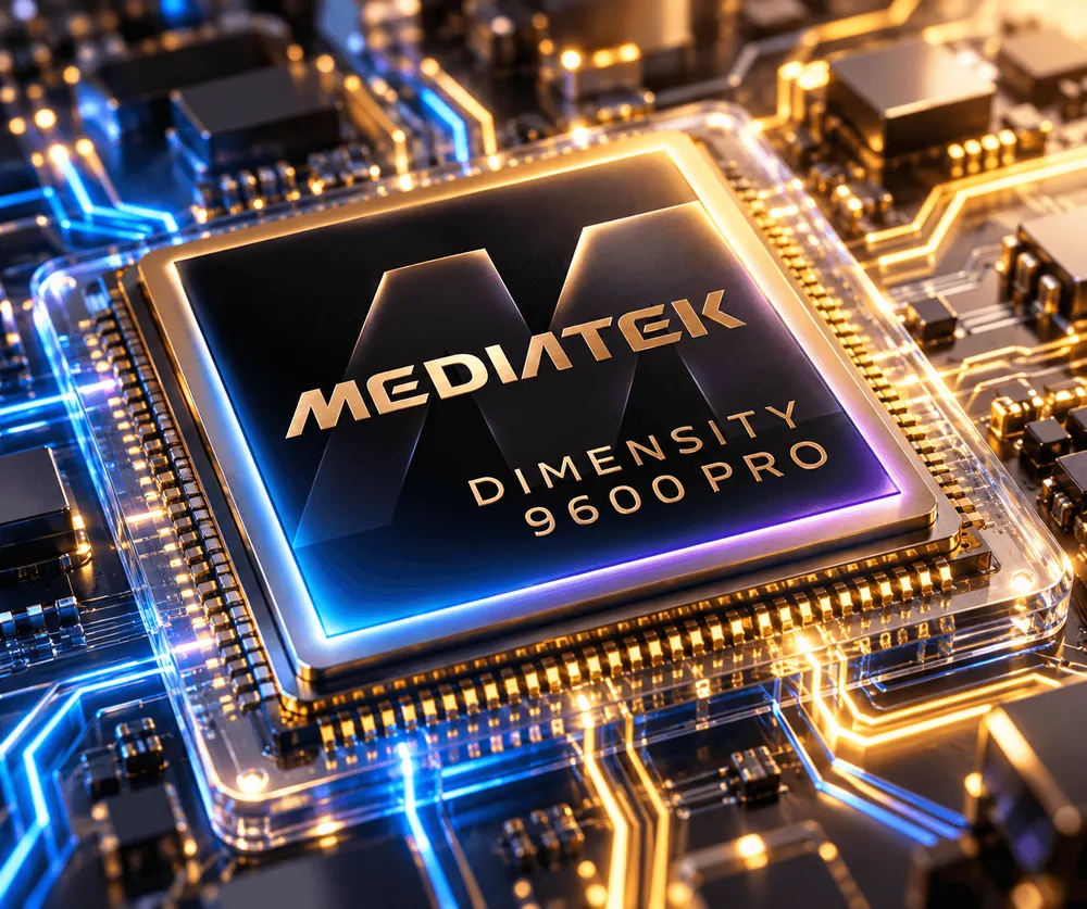
On September 15, 2026, MediaTek officially unveiled its next-generation mobile processor flagship, the "Dimensity 9600 Pro," alongside the mainstream flagship "Dimensity 9600M." Manufactured using TSMC's 2nm process, both chips feature a new design intended to fully exploit the advantages of the cutting-edge node. AI processing on smartphones is shifting from one-off generative tasks that respond to explicit user input toward agentic AI that continuously monitors context in the background and acts autonomously. Anticipating this paradigm shift, the Dimensity 9600 Pro integrates fully upgraded CPU cores, early adoption of a high-speed memory standard, a dual-NPU division of labor, and hardware-level privacy protection. Rather than chasing a single performance metric, the chip reveals a comprehensive architecture designed to boost effective processing capability per watt.
A 2+3+3 All Big Core Design and 34.5MB Cache Deliver the Processing Foundation
MediaTek's ongoing effort to eliminate efficiency cores has reached a new stage with its fourth-generation All Big Core design. The Dimensity 9600 Pro's CPU cluster adopts a three-cluster 2+3+3 configuration unified around the new-generation Arm C2 architecture. It houses two ultra-large "Arm C2-Ultra" cores clocked at up to 4.55GHz, each paired with a dedicated 2MB L2 cache. The middle tier consists of three high-performance "Arm C2-Pro" cores running at 4.35GHz, each allocated 1MB of L2 cache. A third cluster handling baseline clock duties packs three more Arm C2-Pro cores set to 3.10GHz, each connected to a 512KB L2 cache. By eliminating efficiency cores while grading clock speeds and cache sizes across tiers, the design achieves both rapid responsiveness to fine-grained load fluctuations and power efficiency.
Supporting this unconventional cluster design is a massive cache hierarchy totaling 34.5MB. The L2 cache shared across the entire CPU cluster reaches 8.5MB, a substantial expansion from the previous generation. This is complemented by a 16MB L3 cache that absorbs high-speed data access from each core group, and a 10MB system-level cache (SLC) that mediates data transfers across the entire SoC. This expanded cache capacity significantly reduces the frequency of external memory access.
Renewed external interfaces also contribute to the overall boost in processing capability. The chip adopts the next-generation LPDDR6 memory standard, supporting data transfer rates of up to 10,667MT/s. This secures far greater memory bandwidth than the previous LPDDR5X, easing bottlenecks associated with reading weights for large-scale neural networks. For storage, it supports the next-generation UFS 5.0 standard, doubling the theoretical read/write speed compared to the prior generation.
The combination of these design innovations and the physical characteristics of TSMC's 2nm process has yielded, according to MediaTek's internal measurements, up to a 17% improvement in single-core performance compared to the previous flagship generation, along with a 37% reduction in power consumption at equivalent performance levels. Multi-core performance improved by up to 15%, while power consumption saw a dramatic reduction of up to 61%. Beyond simply chasing peak benchmark scores, this reflects a clear emphasis on suppressing thermal runaway during sustained heavy workloads and maintaining practical processing capability.
Dual-NPU and AISeal Support Always-On Agentic AI
At the core of the Dimensity 9600 Pro's AI architecture lies a Dual-NPU configuration that packs two AI processors with distinct roles onto a single chip. MediaTek has physically separated the main system handling heavy inference workloads from the standby system that continuously monitors environmental changes.
The "NPU 1090," responsible for advanced inference, doubles INT4 computational performance compared to the previous generation through enhancements to its quantized computation pipeline. LLM prefill performance, which governs input processing for large language models, improved by 51%, while power efficiency during generation improved by 55% per token. Combined with LPDDR6's wide bandwidth, these computational resources enable fully on-device execution of MoE (Mixture of Experts) models with up to 30B parameters, without relying on the cloud. The chip directly accelerates the MoE structure, which switches between small specialized networks, enabling complex contextual understanding entirely on-device.
Meanwhile, the "Super Efficient NPU 2.0," specialized for low power consumption, supports the always-on awareness functions essential to agentic AI. It monitors microphone audio, camera preview feeds, and various sensor data around the clock while cutting power consumption by 40% compared to the previous generation. It can detect changes in user context and instantly trigger necessary agent processes while keeping the main processor and the high-output NPU fully dormant.
Given the growing frequency with which devices handle personal information and behavioral history, the hardware security foundation has also been thoroughly strengthened. The chip includes a Hardware Root of Trust (HWRoT) that verifies the integrity of the system's foundation, along with a memory isolation technology called "AISeal" built on a pKVM (Protected KVM) hypervisor. This confines private data processed by AI within a protected region completely isolated from the OS and regular applications, blocking the risk of external leakage. To guard against future decryption threats, the chip also incorporates post-quantum cryptography (PQC) acceleration, securing the long-term safety of communications and data storage.
185fps Gaming and the World's First H.266 Hardware Decoder
The GPU handling graphics processing adopts the latest "Arm Mali-G2 Ultra NX" architecture. Peak rendering performance improved by 27% compared to the previous generation, while power efficiency under heavy load improved by 24%. Hardware ray tracing performance, which enhances the realism of game rendering, increased by up to 18%, and the chip supports OMM (Opacity Micromap) ray tracing, which reduces the rendering load of semi-transparent objects. When paired with a device featuring appropriate thermal design, the chip enables high-frame-rate gameplay of up to 185fps in supported titles.
The image signal processor (ISP) overseeing camera and video input is the "Imagiq 1290." It supports 4K240 capture, enabling native ultra-slow-motion recording at 240 frames per second, capturing intricate detail even in rapidly moving subjects. To preserve tonal detail in high-contrast environments, it integrates LOFIC and UFCC technologies to support 17EV of wide dynamic range HDR. For video production, it offers 4K120 Cinematic LOG recording, combined with 4K60 AI True Color Tone, which dynamically optimizes color at 60 frames per second using AI, and subject-tracking autofocus running at 60 frames per second, delivering a shooting environment robust enough for professional use.
In the realm of media playback, the chip is the first smartphone SoC in the world to feature a hardware decoder for the next-generation video codec "H.266 (VVC)." Compared to prior-generation compression technology, it can reproduce equivalent image quality using half the data volume, substantially reducing data usage and battery consumption during high-definition streaming. The display pipeline fully supports the film industry's wide color gamut standard BT.2020 (Rec. 2020) and is also equipped with a tri-fold-ready Tri-port MIPI interface, anticipating multi-screen foldable devices.
The network modem supports 5G-Advanced compliant with 3GPP Release 17. It supports 5CC-CA, aggregating five carriers in the sub-6GHz band, leveraging up to 350MHz of bandwidth to secure downlink speeds of up to 7.4Gbps. It also incorporates Triple SIM Triple Active (TSTA) technology, enabling simultaneous standby and data communication across three SIMs, and supports Wi-Fi 7 along with the latest Bluetooth 6.2 standard.
Architectural Contrast: Pro's 2+3+3 vs. M's 1+3+4, and the Memory/Cache Gap
Alongside the flagship announcement, MediaTek also disclosed specifications for the "Dimensity 9600M," a premium-tier SoC manufactured on the same TSMC 2nm process. Despite sharing the same cutting-edge manufacturing process, a clear architectural boundary separates the two models.
While the Dimensity 9600 Pro features a 2nm-generation All Big Core 2+3+3 configuration with 34.5MB of total cache, the Dimensity 9600M uses a 1+3+4 configuration with a more modest total cache of approximately 26MB.
The Dimensity 9600M's CPU adopts a 1+3+4 configuration, combining one Arm C1-Ultra core with a 2MB L2 cache, three Arm C1-Premium cores each with a 1MB L2 cache, and four Arm C1-Pro cores each with a 512KB L2 cache. Its cache hierarchy consists of a 16MB L3 cache plus a 10MB system-level cache (SLC), totaling 26MB—an 8.5MB reduction compared to the higher-end model's 34.5MB.
The distinction between the two models is also strict when it comes to peripheral components. While the Dimensity 9600 Pro is equipped with cutting-edge LPDDR6 memory, UFS 5.0 storage, a Dual-NPU setup (NPU 1090 and Super Efficient NPU 2.0), and Bluetooth 6.2, the Dimensity 9600M is fitted with proven LPDDR5X memory, four-lane UFS 4.1 storage, a single NPU 990, a Mali-G1 Ultra MC12 GPU, and Bluetooth 6.0 for short-range wireless connectivity.
This differentiation reflects MediaTek's strategy of absorbing the rising costs of cutting-edge components while rapidly extending the foundation of agentic AI across devices at different price points. Emerging standards such as LPDDR6 and UFS 5.0 tend to carry elevated procurement costs in their early rollout phase, making full-scale adoption beyond the premium flagship tier difficult. MediaTek has positioned the top-tier Pro to demonstrate the technological pinnacle, while the M—pairing mature memory standards with a highly efficient 1+3+4 cluster—is positioned to drive adoption across a broader range of flagship devices.
The first commercially available smartphones featuring both SoCs are expected to reach the market from various manufacturers between the third and fourth quarters of 2026. However, the performance improvements and power reduction figures announced are based on MediaTek's internal evaluation environment, and actual sustained thermal behavior and battery life in commercial products will depend on each device manufacturer's chassis design. The true test of how far this cutting-edge process and ambitious architecture can transform everyday practical experience will come once commercial devices hit the market.