

How much longer will ASML's monopoly last? Elon Musk responded to this question, which has long simmered in the semiconductor industry, with a mere two-word post on X. Facing the monopoly on EUV lithography systems that has even shaped the business plans of TSMC and Samsung, Musk—who leads Tesla and SpaceX—has been planning a massive semiconductor plant called "Terafab" in Texas, aiming for in-house manufacturing capacity.
"FEL FTW"—Free-Electron Laser, For The Win. Musk posted this on X on August 6, 2026. If there is any potential for this to shake ASML's monopoly, the main driver isn't the technology itself but a shift in thinking that turns the light source from an "equipment component" into "factory infrastructure." The concentrated FEL light source reportedly being considered for Terafab is too large to fit inside a single lithography system, which means sharing across multiple systems could become the premise.
Why the LPP Method Consumes So Much Power, and How the FEL Method Changes the Equation
ASML's current EUV lithography systems use the LPP (Laser-Produced Plasma) method. Inside a vacuum chamber, tin droplets tens of micrometers in diameter are fired at a rate of roughly 50,000 times per second, and a CO2 laser is fired at them to turn them into plasma, generating EUV light at a wavelength of 13.5nm. This method produces light indirectly via an intermediate substance—tin—and only a small fraction of the input power ultimately becomes usable EUV light on the wafer.
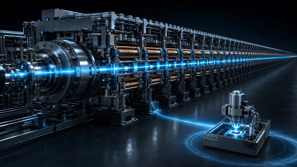
The FEL (Free-Electron Laser) method works on a different principle. A high-energy electron beam is passed through an "undulator," an array of alternating magnets, causing the electrons to oscillate and directly emit EUV light. Because there's no intermediate substance like tin involved, there's no optical contamination from tin vapor, and reportedly less energy is lost during conversion. According to estimates reported by Cailian Press, obtaining 1kW of EUV output requires approximately 4.4MW of input power with the LPP method, whereas the FEL method theoretically requires only about 0.7MW. 36Kr states that under the same conditions, FEL can reduce power consumption to one-quarter to one-fifth of LPP's, and while the reported multipliers vary somewhat, most sources roughly agree on a power-saving factor ranging from several times to around sixfold.
For comparison, ASML's 0.33NA EUV systems consume about 1,170kW, and the next-generation 0.55NA (High-NA) systems are expected to reach about 1,400kW. Against the current reality of a single lithography system continuously consuming this much power, the power savings claimed for the FEL method carry non-negligible implications for massive facilities like Terafab that must supply their own large-scale power. That said, in the concentrated FEL concept reported by Cailian Press, the equipment itself—including the accelerator and undulator—becomes a large-scale installation that wouldn't fit within a typical semiconductor plant. While theoretically the wavelength can be precisely tuned, potentially allowing shortening to below the 6-nanometer range, the sheer footprint of this massive equipment, alongside challenges such as development costs and ensuring reliability for continuous operation, is considered one of the reasons FEL has not been put into practical use for many years.
The Gap Between xLight's 2028 Prototype and Terafab's Mass-Production Plans
Several companies are working on FEL methods or similar next-generation light source technologies. Startups such as TAU Systems and Inversion Semiconductor are also pursuing similar light source technologies using laser-driven compact accelerators. However, no company anywhere has a track record of supplying EUV light sources at mass-production scale, and the company with the most concrete roadmap and government backing is xLight.
For this startup, chaired by former Intel CEO Pat Gelsinger, the U.S. Department of Commerce formally agreed in June 2026, under the CHIPS Act framework, to provide support in the form of acquiring $150 million worth of equity. This makes the government one of xLight's major shareholders. Prior to this, xLight had also raised $40 million in private funding through a venture round led by Playground Global, giving it a development structure built on both government investment and private capital. xLight plans to demonstrate a prototype in 2028 at the Nanotech Complex in Albany, New York.
The $150 million worth of equity the government acquired in xLight is equivalent to roughly ¥23.8 billion at an exchange rate of $1 = ¥159 (as of August 12, 2026). Meanwhile, Terafab's Phase 1 investment is reported at $16.8 billion, or roughly ¥2.67 trillion. A simple comparison shows that the scale of the government's investment in xLight is only about one-hundredth of Terafab's Phase 1 investment. Given this scale of investment and the fact that xLight is a startup with no mass-production track record, it remains uncertain whether, beyond the 2028 prototype demonstration, a mass-production light source actually usable in a factory can be completed.
Construction plans for Terafab are proceeding in Grimes County, Texas, and reporting by TrendForce, based on engineering hiring trends, suggests that memory processes centered on DRAM may come online first. When leading-edge logic processes requiring EUV lithography will actually start up at Terafab has not been officially disclosed, but given that xLight's prototype demonstration is slated for 2028, as long as things proceed according to the current roadmap at minimum, it seems unlikely that an FEL-method EUV light source would be operational at Terafab before then. Bits&Chips, citing anonymous sources, has reported that ASML previously examined FEL technology but chose not to prioritize it, judging that the efficiency gains were limited relative to the high development costs. This suggests a picture in which technology the industry leader was reluctant to pursue is now being revived by the uniquely massive scale of demand that Terafab represents.
When the Center of the Monopoly Shifts: The Light Source Moves from "Component" to "Infrastructure"
ASML's position in the EUV lithography system market is overwhelming. For EUV lithography systems targeting processes at 7nm and below, there is no competitor capable of mass production, and leading foundries such as TSMC and Samsung have no choice but to align their business plans with ASML's supply schedules. One of the premises underpinning this monopoly structure has been the design in which the light source is built into each individual lithography system. The LPP method's CO2 laser and tin droplet generator are designed as an integrated part of the main equipment, and procuring the light source separately from its surrounding optics, masks, and control systems has not been an assumption built into the system.
The concentrated FEL light source reportedly being considered for Terafab is physically enormous and won't fit inside individual lithography systems, suggesting a design in which a single light source is shared across multiple lithography systems within a building (TAU Systems and Inversion Semiconductor are pursuing more compact approaches, so this large scale is not a constraint common to FEL technology as a whole). Even so, this constraint has the potential to upend the very premise that each system contains its own built-in light source. It means the light source's role shifts from a per-system "component" to "infrastructure" shared across an entire factory—and it is precisely because of Terafab's massive scale that this large equipment footprint becomes a premise rather than a barrier.
That said, even if in-house production of light sources is realized, this doesn't mean dependence on ASML disappears. As Cailian Press points out, elements required for lithography—such as optics, masks, and control systems—will continue to rely heavily on ASML's technology regardless of which light source method is used. What could be separated out is just one element among the components of an EUV lithography system: the light source, which happens to be the element that most significantly affects cost and power consumption.
A technical crack is opening up in the "integrated design" premise that has underpinned this monopoly, caused by the physical bulkiness of the FEL light source. What is driving this change is not a business strategy decision. It is a physical constraint—the fact that it doesn't fit inside the equipment—that is forcing the structural shift.
Points of Contact with Japanese Equipment Makers and Energy Costs
Regarding Terafab, contacts with equipment makers such as Tokyo Electron and Applied Materials have been reported by outlets including sbbit.jp, meaning this is already not an unrelated matter for Japan's domestic semiconductor manufacturing equipment supply chain. If adoption of the FEL method becomes a reality, it could also affect demand structures for existing LPP light source-related components, and even Japanese equipment makers that don't handle light sources themselves could be affected—through opportunities to supply surrounding optics, transport systems, and control systems.
There are also points of contact from a power perspective. ASML's High-NA systems are expected to consume about 1,400kW, and rising electricity costs are an issue directly tied to manufacturing costs—something that is not unrelated to domestic semiconductor-related companies either. If the several-fold power savings claimed for the FEL method are demonstrated, it should become a consideration not just for Terafab but also for operators running plants in regions with significant power constraints. However, this only becomes realistic once xLight's prototype is demonstrated in 2028 and subsequent mass production succeeds.
Ultimately, what Musk's two words—"FEL FTW"—signify is not that ASML's monopoly will collapse immediately. Among the candidate companies including xLight, whether the frontrunner can get past the 2028 prototype demonstration, and whether demand at a scale like Terafab's can push forward the mass production that follows, is what the future of EUV light sources shifting from "equipment component" to "factory infrastructure" hinges on.