

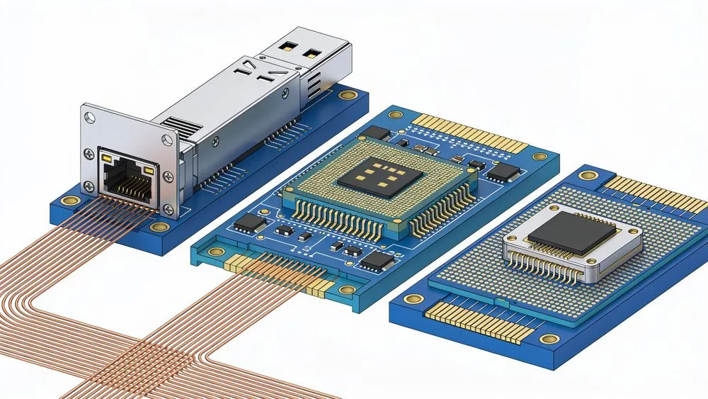
Open a data center rack and you'll see rows of optical transceivers lined up along the front panel of a switch. A switch with 144 800G-capable QSFP-DD modules plugged in is the standard sight in an AI cluster today. But this scene contains a structural waste. The distance from the transceiver on the front panel to the switch ASIC is 15 to 30 centimeters. When a 200G/lane signal travels over this copper wiring, attenuation is significant, forcing a DSP (digital signal processing) chip on the receiving end to regenerate the signal. Of the 14 to 17 watts consumed by a single 800G module, 6 to 8 watts is taken up by the DSP alone. Roughly half the power is spent simply repairing the signal's "journey."
Shorten that distance, and the DSP becomes unnecessary. This idea itself has existed since the mid-2010s. Co-Packaged Optics (CPO)—which mounts the optical engine (the components that convert electrical signals to light) on the same package substrate as the switch ASIC—is a design that fundamentally removes the copper wall. Broadcom has publicly stated that CPO can reduce optical system power consumption by 65 to 70%. For NVIDIA's 1.6T link, a reduction from roughly 30 watts to 9 watts per link has been demonstrated.
In theory, CPO looks like the optimal solution. The problem lies in the manufacturing gap between theory and mass production.
The Reality Exposed by a 19% Yield Figure
In the CPO manufacturing process, optical engines are mounted onto the ASIC's package substrate via reflow (heat-based soldering). The alignment precision required for optical fibers is sub-micron. Redoing an already-mounted engine would require reheating to 220–260°C just millimeters away from the ASIC, and optical fiber alignment cannot withstand a second thermal cycle. In other words, if even one of 32 optical engines is defective, the ASIC, the substrate, and all the remaining engines must all be discarded.
In its June 2026 research note "Powered Down, Lights Off," SemiAnalysis calculated the compound yield assuming a 95% mounting yield per optical engine. . For a 32-engine package, the good-unit rate comes out to about 19%—only 1 in 5 works properly. This figure sent shockwaves through the market. On June 9, in the U.S. market, Applied Optoelectronics (AAOI) fell about 17% in a single day, and Lumentum dropped roughly 8%. Coherent fell about 11%, and Marvell about 7.6%.
GlobalSemiResearch immediately published a rebuttal, pointing out that this calculation ignores screening, binning (sorting processes), and the yield improvements from redundant engines that NVIDIA designed into Spectrum-X. Morgan Stanley, in its June 10 report, did not dispute CPO's underlying technology roadmap, but simply revised its 2027 optical engine shipment forecast downward from a previous range of 20 to 30 million units to 6 to 7 million units.
The crux of the debate is not "whether CPO is viable" but "when and at what scale it can be used." SemiAnalysis pushed back scale-out-oriented CPO shipments to 2027 and full-scale mass production to 2028–2029. This shift in timeline opened a window for a different architecture.
The Optical Engine Left in the Socket: NPO's Design Philosophy
Near-Packaged Optics (NPO) sits between CPO and pluggables. Rather than mounting the optical engine on the ASIC's package substrate, it places the engine on a separate engine board positioned immediately adjacent to the ASIC. The electrical wiring length shrinks from centimeters to just a few millimeters, eliminating the need for a DSP. However, there is one decisive difference from CPO: the engine connects via a socket and can be swapped in the field.
| Pluggable | NPO | CPO | |
|---|---|---|---|
| Optical engine location | Front panel (15–30cm from ASIC) | Independent board near ASIC | Same package substrate as ASIC |
| DSP | Required (6–8W/800G) | Not required | Not required |
| Field replaceable | Yes | Yes | No (reflow-mounted) |
| Impact of single-unit failure | That module only | That socket only | ASIC + substrate + all engines discarded |
| Optical system power per 800G | 14–17W | ~5–7W (estimated) | ~4–5W (per Broadcom) |
In an X thread on August 10, SemiAnalysis organized NPO's advantages into three points: field-replaceable serviceability, a blast radius for failures limited to a single socket, and simpler assembly since the optical engine sits on a separate package from the ASIC. This is a structure that preserves most of CPO's performance benefits while avoiding its manufacturing and reliability challenges.
At OFC in March 2026, Broadcom unveiled a 3.2T VCSEL-based NPO product line. According to the company's blog, this NPO engine's energy efficiency is about 1 pJ/bit. Compared to silicon photonics approaches, which typically run 5 to 10 pJ/bit, that's a 5-to-10x efficiency advantage. With 18 engines arranged, escape bandwidth density reaches over 0.6 Tbps/mm, with total escape bandwidth hitting 73.7 Tbps (at 128 Gbps/channel). VCSELs have decades of mass-production track record, with field-proven failure-in-time (FIT) rates reported at below 0.1.
Standardization and Mass Production Gears Start Turning Together
Even a superior architecture won't spread without an ecosystem. On March 12, 2026, timed with OFC, six companies—Ciena, Coherent, Marvell, Molex, Samtec, and TeraHop—established the Open CPX MSA (Co-packaging Multi-Source Agreement). Its goal is to define a common specification for socketed optical engine interfaces covering both NPO and CPO. It standardizes connector mechanical structure, thermal design, electrical pin layout, and management interfaces to ensure multi-vendor interoperability.
At the launch announcement, LightCounting CEO Vladimir Kozlov stated that "annual port shipments are projected to exceed 100 million within five years," contrasting this with CPO/NPO shipments of under 1 million ports as of 2025. Achieving over 100x growth is not possible without standardization.
Demand-side momentum is also building. In a May 2026 IPEC webinar, Alibaba revealed it had completed beta testing of 3.2T NPO and planned to begin pilot operations in Q3 of the same year. Its target for 6.4T NPO alpha samples is to complete system-level debugging by September 2027. Tencent has also finished verification of both 3.2T VCSEL NPO and silicon photonics NPO, and plans a Q4 2026 pilot deployment. Ranovus has reportedly already shipped NPO modules to a U.S. cloud company, though the public announcement is expected to wait until OFC 2027.
On the supply chain side, Foxconn Interconnect Technology has been mass-producing solderless LGA-to-LGA sockets and pluggable laser source cages for Broadcom's Bailly since May 2025. Placing the laser outside the package is the mainstream design for both CPO and NPO, with OIF's ELSFP specification (a hot-swappable external laser module), established in August 2023, serving as the common foundation.
Why NVIDIA's "CPO" Carries NPO Characteristics
NVIDIA's Quantum-X Photonics InfiniBand switch began full-scale deployment in 2026. It achieves 144 ports of 800G using 18 silicon photonics engines, with 18 removable external laser modules supplying the light. NVIDIA calls this "CPO."
However, a structure where the engines can be bolted off the package and the lasers slide out from the front panel is precisely the serviceability characteristic that SemiAnalysis attributes to NPO. In a July 2026 research note, LightCounting confirmed the industry consensus that CPO and NPO will coexist, noting that if NVIDIA offers NPO as an option, it could shorten development cycles and potentially see an initial deployment as early as next year.
Broadcom is rolling out both architectures in parallel. Its 51.2T Bailly CPO switch has been in mass production at Micas Networks since 2024. The 102.4T Tomahawk 6 Davisson began customer shipments in October 2025. In addition, Broadcom offers a separate 3.2T VCSEL NPO for "customers seeking density without a soldering commitment."
Reliability verification at Meta is also progressing. Broadcom's CPO system recorded zero link flaps (momentary outages) during a cumulative 1 million hours of 400G-equivalent port time in Meta's high-temperature lab environment. Broadcom announced this in October 2025, with details reported at that year's ECOC and at OFC 2026. At OFC 2026, Meta presented the standard that "for optical technology to be attractive, it must deliver reliability and performance at cost and power efficiency comparable to electrical solutions."
The Timeline Set by TSMC's COUPE
How long NPO's "interim period" lasts depends heavily on the progress of TSMC's COUPE (Compact Universal Photonic Engine) platform. COUPE is a technology that directly stacks electrical dies and photonic dies using SoIC stacking, physically minimizing inter-die impedance. The first-generation pluggable form is set to enter mass production in 2026. The second generation targets a 6.4T CPO form around 2027. In the third generation, the optical system will be fully integrated inside the processor package.
TSMC's COUPE bandwidth density roadmap depicts an 8x improvement over four years, from 0.5 Tbps/mm in 2026 to 4 Tbps/mm in 2030. If this schedule is realized, NPO's role would be confined to a 2-to-3-year transitional period.
However, if SemiAnalysis's 2029 full-scale mass production scenario turns out to be closer to reality, NPO will continue to carry demand through the end of the decade. In that case, further strain would be placed on a photonics supply chain where laser and packaging capacity are already tight. At the OCP APAC Summit, ASE's Nicole Tien stated that the wafer-level test standards and simulation frameworks needed to generalize CPO for a multi-vendor market do not yet exist. NVIDIA's CPO mass production is the product of deep, bilateral co-development with TSMC, and the conditions for extending that achievement to the industry as a whole are not yet in place.
There is little major disagreement in the industry that CPO represents the ultimate form of optical interconnects. The question is who will walk the path to get there, when, and at what scale. NPO is emerging on production lines as the most concrete answer to that question at this moment.