

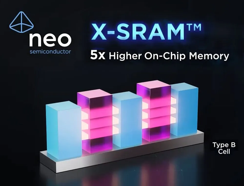
In AI computing, HBM, where model data resides, and on-chip SRAM, which operates at high speed near the compute units, each represent separate capacity bottlenecks. On August 4, NEO Semiconductor announced "NEO.AI," which addresses both through X-SRAM and 3D X-DRAM. The substance of this announcement is that the newly disclosed X-SRAM and the 3D X-DRAM—whose silicon PoC was announced in April—have been brought together on a common platform. However, no product specifications or shipment plans were presented, and inconsistencies remain between official materials regarding the capacity multipliers.
Addressing Two AI Memory Bottlenecks on a Single Platform
What NEO.AI separately addresses is on-chip AI cache and HBM capacity. The former corresponds to SRAM located near the compute units, while the latter corresponds to high-bandwidth memory that holds model data. Even if capacity is increased for one, the bottleneck in the overall memory hierarchy of AI accelerators will not disappear if the constraint on the other remains. NEO has assigned X-SRAM and 3D X-DRAM to these two areas respectively and proposed them as a platform.
The company's announcement is not about replacing memory as a single type of component. It targets different design problems: on-chip cache, which uses area on a planar surface, and HBM, which increases capacity through stacking. Therefore, one cannot read this as meaning that adopting NEO.AI would replace existing HBM or SRAM already installed in GPUs. What the published materials show is a technical foundation and pathway toward commercialization.
X-SRAM Aims to Expand On-Chip AI Memory Capacity
X-SRAM is a technology that NEO describes as using a new 2-transistor cell configuration, in contrast to conventional SRAM, which uses 6-transistor (6T) cells. The company claims that its current 2D design achieves up to 5x the density of conventional SRAM, SRAM-class performance, and compatibility with advanced nanosheet CMOS processes. However, this is NEO's maximum density claim and does not mean that AI accelerators become 5x faster.
The company's technology page states that current on-chip AI memory (SRAM) sits at 200–400MB, and that X-SRAM makes 1–2GB possible. This capacity figure is also not a measured value from an implemented chip, but rather a target set forth by the company. The FMS 2026 agenda includes a statement that SRAM can occupy 40–70% of the die area in advanced processors, along with a description of 5–10x on-chip density via NEO.AI, but both figures are based on the event page and company-provided materials, not independent benchmarks.
Furthermore, NEO also presents a roadmap for a future 3D X-SRAM that would expand on-chip AI memory capacity by 20–40x. At present, what is publicly available is a description of 2D X-SRAM; silicon demonstration of X-SRAM, measured performance, the implementation conditions that determine capacity, and commercialization timing have not been disclosed.
3D X-DRAM Stacks HBM Capacity Vertically
3D X-DRAM is a concept that leverages 3D NAND manufacturing processes to stack DRAM. NEO presents three cell lineages: 1T0C, 1T1C, and 3T0C. The 1T1C and 3T0C use IGZO, and since 3T0C employs current sensing, the company explains that it is suited for in-memory computing and AI applications. The aim of increasing capacity vertically differs from that of X-SRAM.
The silicon PoC announced in April is a result from a prototype chip that NEO reported in its company announcement, for which the cell type, number of layers, and array scale were not disclosed. Therefore, the following figures cannot be regarded as measured values covering all three types—1T0C, 1T1C, and 3T0C—together. According to NEO, read/write latency was under 10ns, data retention at 85°C exceeded 1 second, bit-line/word-line disturb at 85°C also exceeded 1 second, and endurance exceeded 10^14 cycles. For data retention, the company compares this to JEDEC's 64ms standard. The PoC was co-developed with NYCU IAIS and manufactured and tested at NIAR-TSRI using existing 3D NAND infrastructure. NEO states that it also used existing equipment, materials, and processes.
What can be confirmed here are the electrical characteristics and reliability behavior of the prototype chip. These are not measured values indicating HBM module capacity, multi-layer array yield, price, power consumption, heat dissipation, or adopting customers. The sub-10ns, over-1-second, and over-10^14-cycle figures obtained from the PoC cannot be linked to the capacity multiplier of 3D X-DRAM.
Conditions for Mass Production That Remain Beyond the PoC
If existing 3D NAND-derived infrastructure and processes can be utilized, this offers a different path than building a new manufacturing foundation from scratch. Even so, what determines mass-production viability is array-level implementation, multi-layer test chips, and yield. NEO itself has cited the development of these elements and discussions with partners as the next stage following the PoC, stating that it will pursue licensing and partnership models. The adopting parties among memory makers, foundries, and AI accelerator vendors, as well as the timing of availability, remain undetermined.
There are also points to clarify regarding the capacity claims. The August 4 announcement claims up to 10x the capacity of conventional DRAM for next-generation HBM. Meanwhile, the FMS 2026 agenda and NEO's 3D X-DRAM page each state up to 8x in their respective platform descriptions. Since the denominator, configuration, and measurement basis have not been disclosed, these two figures cannot be reconciled into a single confirmed specification. The 10x figure should be treated as the maximum claim stated in the announcement, not as a measured or guaranteed value.
The 2025 white paper also includes figures such as up to 512Gb for a specific 1T1C design, retention exceeding 450 seconds, and an HBM bus width of up to 32K bits via hybrid bonding. These are figures related to design and simulation, existing on a different layer from the 2026 silicon PoC. Evaluating NEO.AI as a mass-production technology will require, in addition to clarifying the comparison conditions for capacity multipliers, results covering power, heat, yield, and cost in multi-layer arrays.