

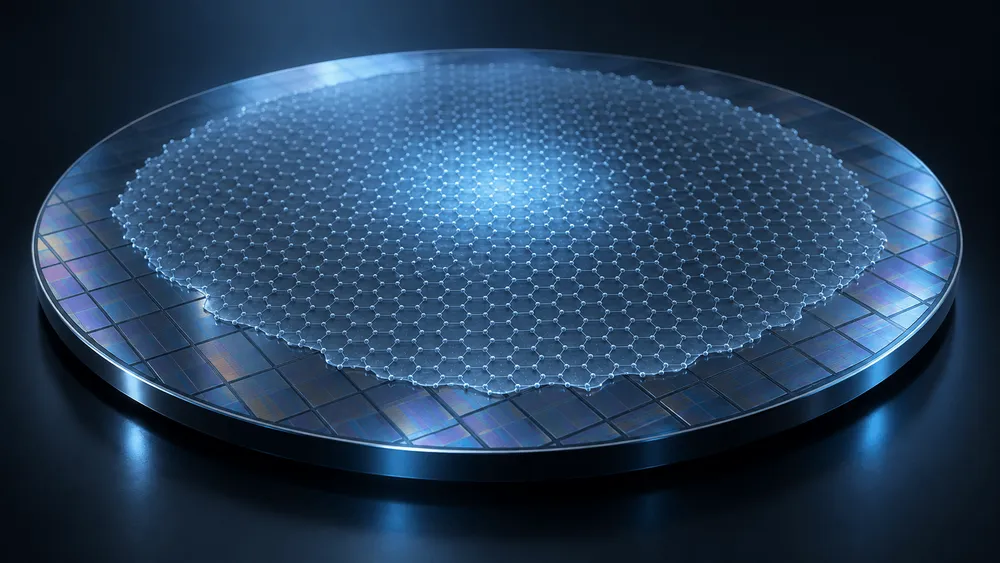
Singapore startup Nexstrom announced on September 22, 2026 that it has raised $12 million (about ¥1.88 billion) in a seed round led by Xora Innovation. The money will go toward commercializing "North Star," a tool that grows TMDs (transition metal dichalcogenides), the material for 2D semiconductors, directly on 300mm (12-inch) wafers. In June 2026, ASML, TSMC, and imec demonstrated 2D-material transistor integration on 300mm wafers, but the channel had been grown on a separate substrate and then transferred. Can a film of the quality a production line demands be grown uniformly, directly on the wafer? That is the one question Nexstrom is trying to answer. Comparing the company's materials with its executives' statements also reveals a difference in timing: is the 300mm milestone "achieved" or "due to be completed by the end of October"?
Of $15 Million in Total Funding, 20% Is Non-Dilutive
Xora Innovation led the round, with Foothill Ventures and SEEDS participating. According to the company, cumulative funding stands at $15 million (about ¥2.36 billion), of which $3 million is non-dilutive.
Non-dilutive funding is money received without giving up equity, such as a grant. Of the $15 million total, the $3 million, or 20%, is non-dilutive. The source has not been disclosed, and neither the valuation nor each investor's contribution has been made public. Yen conversions use ¥157 to the dollar (as of September 22, 2026).
Nexstrom is also a company created by investors. The timeline on its official website says Lance Li and Xora Innovation founded the company in 2024. It was born within Xora's venture-building framework, in which an investment firm is involved from the earliest stage of a business. Xora is reported to be a VC under Temasek. Participant SEEDS is a state-affiliated investment entity belonging to SG Growth Capital, the investment arm of Enterprise Singapore and the EDB (Singapore Economic Development Board).
The management team is lined with people who did research at TSMC. CEO Dr. Phoebe Tan is a co-founder, and Chief Scientist Dr. Lance Li led research on post-silicon electronic devices at TSMC. Dr. Li has worked on CVD (chemical vapor deposition) of single-crystal MoS2 (molybdenum disulfide) since 2012, and the press release says he has been named a Clarivate Highly Cited Researcher since 2018. Board advisor Prof. Philip Wong of Stanford University served as TSMC's vice president of research from 2018 to 2020.
What this lineup sells is equipment for growing chip materials, not the chips themselves. According to the EDB, Singapore accounts for one in ten of the world's semiconductors and one in five pieces of semiconductor equipment. Nexstrom does not position itself as a competitor to foundries; it stands on the side that supplies materials and equipment. With a state-affiliated investor on board, it has started out as an equipment company in a country where the equipment industry is concentrated.
Why a Crystal Under 1nm Thick Is a Candidate to Succeed Silicon
To shrink a transistor, the channel through which current flows must also be made thinner. According to imec, when a silicon channel drops below 10nm in thickness, mobility (how easily electrons move) and on-current fall sharply. TMDs are crystals in which metals such as molybdenum and tungsten form layers with sulfur or selenium, and a single layer is only about 0.7nm thick.
A channel even thinner than the thickness at which silicon loses performance can be made from the crystal's own thickness. That property is why TMDs are named as candidates for next-generation channels. XenoSpectrum covered the basics of short-channel effects in an article on research into transfer-free growth of MoS2 wafers.
But being thin alone does not make a transistor. A review by Das et al. published in Nature Electronics in 2021 pointed out that even the best TMDs have contact resistivity with metals roughly one order of magnitude higher than heavily doped silicon. imec's Gouri Sankar Kar also explains that with 2D TMDs, a large contact area has so far been needed to lower contact resistance, which has hindered scaling.
Another barrier is the film itself. Intel's Kevin O'Brien said in an October 2024 Semiconductor Engineering article that 2D semiconductors cannot be mass-produced without better and more consistent film quality. In the same article, CEA-Leti explained that the best CVD films are grown on substrates such as sapphire at temperatures above 600°C. A high-performing film may exist, but that does not mean it will grow with the same quality everywhere across a full silicon wafer.
Nexstrom is aiming at the film side of these two barriers. In the press release, Dr. Li said, "The challenge is not demonstrating the potential of 2D materials, but manufacturing them at the scale and quality that leading-edge foundries demand," and Prof. Wong commented, "The industry needs high-quality, uniform 2D materials on 300mm substrates." The contact-resistance problem remains an area the company's tool does not directly address.
"Achieved at 300mm" vs. "12-Inch by End of October": Two Tenses From One Company
The product, North Star, is a tool that grows TMDs directly on 300mm (12-inch) wafers. The official website describes it as a cold-wall CVD system and says the company extended its MOCVD (metal-organic chemical vapor deposition) platform to 100mm wafers in 2025. The question is how far along the 12-inch stage is beyond that.
Lining up the company's own statements, the tenses do not match. The company overview in the press release says it "has developed" the industry's first platform for producing 12-inch single-crystal 2D semiconductors, in the completed tense. Yet the body of the same release also contains a progressive statement, "driving toward the industry's first 12-inch 2D wafer growth." The 2026 entry in the official website's timeline says it "achieved commercial-grade TMD synthesis on 300mm wafers."
CEO Phoebe Tan described a different stage to TechCrunch. She said the company had obtained on-wafer material results with a newly installed 12-inch tool, and, describing a process that has been widened step by step from 2 inches to 6 inches, said, "8-inch and 12-inch are expected to be completed by the end of October." In other words, while the press release and website say TMD growth at 300mm has been achieved, the CEO speaks of completing the 12-inch process as scheduled for the end of October 2026.
The two statements can coexist. Obtaining a feel for the material on a 12-inch tool and completing the 12-inch process may refer to different stages.
Still, what readers can take from this is only that the 12-inch tool has started running and produced material results. The company's CEO herself has not said that a process to stably grow production-grade film at 300mm is complete. No third-party quality evaluation of 300mm wafers has been published. According to TechCrunch, some companies in the industry are testing samples, but their names have not been disclosed.
The expression "industry first" also needs a caveat. MIT spinout CDimension announced 2D material growth across a full 300mm wafer in July 2025. Whether the claim holds depends on the criteria for "first," such as whether the material must be single-crystal.
The performance figures share the same pattern. The official website lists "up to 100x lower defect density," "up to 75% lower switching power," and "more than 2x gate-length scaling," but does not state what they are compared against, or at what wafer diameter and measurement conditions they were obtained. The meaning of the numbers changes greatly depending on whether the baseline is silicon or TMD films made by other growth methods. For now, these can only be read as the company's claims.
1000°C, 300°C, 200°C: Three Routes to Put a Film on a Wafer
In June 2026, ASML, TSMC, and imec announced that they had built n-type transistors (nFET) using MoS2 and p-type transistors (pFET) using WS2 and WSe2 on the same 300mm wafer. The contacted poly pitch (CPP), the spacing between gate electrodes, was 50nm, and 94% of the transistors worked. For the channel material, films grown elsewhere were transferred onto a wafer processed with trenches pre-filled with tungsten. The path to 300mm integration shown jointly by the industry's three main players was transfer, not direct growth.
The reason transfer is chosen is temperature. According to imec, growing 2D materials directly on a wafer normally requires about 1000°C. The transfer step that moves a film grown on another substrate, by contrast, takes only about 300°C.
BEOL (back-end-of-line) processing that builds the wiring layers, and wafer backside processes, must be kept below 400°C so as not to damage devices already built. If growth at 1000°C were performed on a partially finished wafer, the circuits underneath could not withstand the heat. Hence the division of labor: high-temperature growth is done elsewhere, and the film is brought in by low-temperature transfer.
MIT spinout CDimension is trying to break down this barrier from the temperature side. In July 2025, the company announced a proprietary process that grows a monolayer of MoS2 across a full 300mm wafer at about 200°C, claiming it could halve the time to commercialization. The announcement, reported by IEEE Spectrum, is a claim that growth temperature has been brought within the BEOL constraint of below 400°C.
Lining up the published routes gives the following. Temperatures are representative values given by each source and were not measured under the same conditions.
| Route | Published temperature | Status at 300mm | Source |
|---|---|---|---|
| Direct growth (general) | About 1000°C | Not stated | imec |
| High-quality CVD film (on substrates such as sapphire) | Above 600°C | Not stated | CEA-Leti (October 2024) |
| Grown on separate substrate, then transferred | About 300°C (transfer step) | ASML, TSMC, and imec integrated 50nm-CPP n-type and p-type devices, 94% working (June 2026) | imec |
| CDimension low-temperature direct growth | About 200°C (company claim) | MoS2 monolayer across full 300mm (announced July 2025) | IEEE Spectrum |
| Nexstrom North Star | Not disclosed | Advertises direct growth at 300mm; 12-inch process due to complete at end of October | Company, TechCrunch |
| Reference: upper limit for BEOL and backside processes | Below 400°C | Not stated | imec |
Among the routes for putting 2D materials on a wafer, direct growth normally takes about 1000°C, growing on a separate substrate and transferring takes about 300°C, and CDimension's low-temperature growth takes about 200°C, while Nexstrom advertises direct growth at 300mm but has not disclosed its growth temperature. Nexstrom's row is the only one with no value in the temperature column. Depending on the temperature at which Nexstrom's film grows, it will either be something that can be placed directly on wafers with devices already built, or a front-end supplier whose film is grown on a separate substrate and transferred.
Nexstrom and CDimension stand on the same side in selling "growing directly on the wafer." The difference is the axis of disclosure. CDimension puts temperature up front, while Nexstrom puts the 300mm diameter and single-crystal quality up front. What Dr. Li has worked on since 2012 is the growth of single-crystal MoS2, and the company's focus on quality uniformity is consistent with that background.
Will a 12-Inch Tool Make It in Time for the Early-2030s Adoption Window?
TechCrunch reports that Nexstrom expects its tool to be ready for commercial production between 2030 and 2035. Placing this timing on the same calendar as the company's and the industry's milestones gives the following.
| Timing | Event | Source |
|---|---|---|
| 2012 | Lance Li's group reports CVD growth of single-crystal monolayer MoS2 | Li lab website |
| 2024 | Lance Li and Xora Innovation found Nexstrom | Company website |
| 2025 | MOCVD platform extended to 100mm wafers | Company website |
| July 2025 | CDimension announces 300mm MoS2 growth at about 200°C | IEEE Spectrum |
| June 2026 | ASML, TSMC, and imec announce 50nm-CPP 2D transistors at 300mm (transfer method) | imec |
| September 22, 2026 | Nexstrom announces $12M seed round | Company press release |
| End of October 2026 (planned) | 8-inch and 12-inch processes to be completed | TechCrunch (CEO statement) |
| Around 2030 | A7 node on imec's roadmap; 2D materials to be introduced first in peripheral devices at A7 | Tom's Hardware (2023 report), imec |
| 2030–2035 (expected) | Nexstrom's tool ready for commercial production | TechCrunch |
| Through 2036 | Atomic-scale channels at A5–A2 nodes | Tom's Hardware (2023 report) |
Nexstrom widened its wafer diameter from 2 inches to 6 inches in the two years since its 2024 founding and has set completion of its 8-inch and 12-inch processes for the end of October 2026, but it expects commercial production readiness in 2030–2035, which overlaps with the period when imec said 2D materials would be introduced into peripheral devices starting at the A7 node (around 2030). imec has indicated that it will begin using 2D materials not in the channels of the most advanced transistors first, but in peripheral devices such as planar transistors placed in the BEOL or on the wafer backside. The A7-around-2030 timing comes from a 2023 roadmap report and may have been revised since.
Read together with the earlier table, this overlap comes with one condition. The BEOL and backside that imec names as first applications are precisely the places subject to the below-400°C constraint. To bring directly grown film there, it must either be grown at low temperature or combined with transfer. Because Nexstrom's growth temperature has not been disclosed, whether its tool can enter the first adoption window cannot be judged from current materials.
There are also factors that could push the timing itself back. In October 2024, imec's Kar pointed out that the CFET (a structure stacking nFET and pFET vertically) could extend silicon scaling by up to 20 years. If silicon is prolonged, demand for the most advanced nodes using 2D materials in the channel could be pushed off by that much. The consistency of film quality that Intel's O'Brien cited as a prerequisite for mass production is an item on which no third-party evaluation data for Nexstrom has yet been published.
There are three things to watch, in near-term order. Can the company show that it completed the 8-inch and 12-inch processes on schedule at the end of October? Will it disclose its growth temperature and the baseline for its performance figures? Will the names of the companies testing samples, or their evaluation results, come to light? If all three come together and a third party confirms that uniform single-crystal film can be reproduced across a full 300mm wafer, foundries would gain one external source of 2D material, and a candidate to supply materials for the phased adoption imec envisions in the 2030s would appear in the form of a concrete tool.