


The natural assumption is that smaller things are easier to build quickly. As the distance between components shrinks, design and mass production would seem to get simpler, not harder.
Yet NTT's roadmap tells a different story. Optical wiring between GPU boards is headed toward commercialization in fiscal year 2026, but the wiring between semiconductor packages further down the line is still in the prototype stage, and the connections between individual dies inside those packages aren't expected until around 2032. The shorter the distance, the further out the timeline stretches. Tracing the reasons reveals that the precision required to manufacture components changes dramatically depending on just how small the target gets.
Why a telecom company is bringing optical wiring to GPU boards in FY2026
ASICs used in AI data center switches can consume more than 500W each. According to a technical explainer from the NTT Technical Journal, roughly 30% of that power goes to I/O circuits that transmit high-speed electrical signals. The faster and further a signal needs to travel, the more electricity bleeds off as heat along the way. This is a physical limitation of electrical wiring itself, one that no amount of clever semiconductor design can eliminate.
As a way past this wall, NTT announced its photonics-electronics convergence switch, PEC-2, on October 6, 2025, paired with a Broadcom ASIC and a chassis from Taiwan's Accton. The switch offers a total transmission capacity of 102.4Tbps and houses 16 PEC-2 devices. Traditionally, pluggable optical transceivers sat at the front of a switch, connected to internal chips via electrical wiring. PEC-2 instead replaces that entire electrical link with a new optical device mounted right next to the chip. This approach is known as Co-Packaged Optics (CPO).
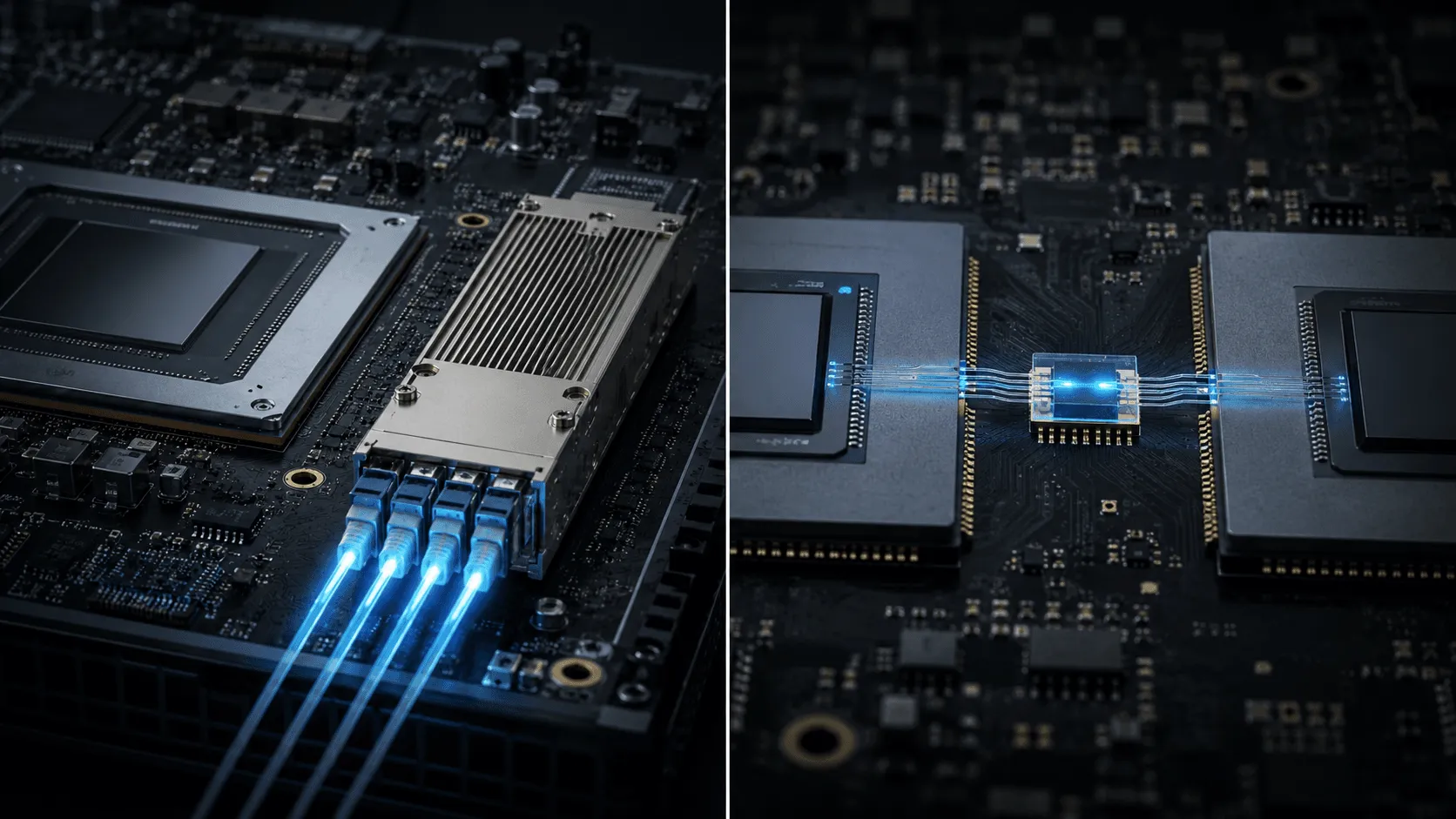
The effect shows up clearly in the numbers. According to the NTT Technical Journal, compared to eight conventional pluggable transceivers at 12W each (96W total), PEC-2 achieves the same function at just 48W—a 50% reduction. NTT has stated plans to supply commercial samples of PEC-2 during fiscal year 2026, and a prototype already ran for six months at the 2025 Osaka-Kansai Expo, routing video data to GPUs for AI video analysis.
PEC-2 can hit its FY2026 target because its target is still wiring between components on a circuit board—connections larger than a millimeter. The stages that follow, PEC-3 and PEC-4, shrink the target further into the interior of ever-smaller components. How small the target gets is what determines how fast each subsequent stage can move.
Why package-to-package optical wiring can't arrive until 2028
PEC-3 targets wiring even smaller than PEC-2's. This is the wiring that connects one semiconductor package to another—CPU to GPU, for instance—and NTT calls it "optical I/O." According to a technical explainer from EE Times Japan, commercial samples aren't expected until 2028, with practical deployment around 2030. That's several years behind PEC-2's FY2026 commercialization target.
The reason lies in the sheer difference in scale between what PEC-2 and PEC-3 are trying to achieve. PEC-2 converts wiring between components sitting on a circuit board into optical links. PEC-3's optical chiplet, by contrast, aims to pack 16 thin-film optical devices—what the NTT Technical Journal calls "membrane devices"—onto a substrate measuring just 1.11mm by 2.75mm, roughly the size of a fingernail. According to EE Times Japan's technical explainer, this optical chiplet is designed to directly connect CPU and GPU semiconductor packages to each other.
What makes membrane devices so hard to miniaturize is that silicon alone can't efficiently produce lasers or optical modulators. The solution requires bonding thin films of indium phosphide-based compound semiconductors—materials known for their light-emitting properties—directly onto a silicon substrate. The process of bonding two materials with very different properties into thin films without damaging either demands a level of integration precision entirely different from what PEC-2's board-level components require.
Both are described with the same phrase, "optical wiring," but PEC-2 deals with components sitting on a circuit board, while PEC-3 deals with the gap between semiconductor packages small enough to fit on a fingernail. At this scale, an entirely new thin-film device combining different materials has to be built from scratch—work that accounts for the timeline stretching to 2028 for initial samples and around 2030 for practical deployment.
2032: reaching the space between dies
Beyond PEC-3 lies the wiring that connects die to die. Inside a semiconductor package, multiple dies—the actual etched circuit elements—sit side by side, and connecting the wiring inside that package optically is the job of "PEC-4," expected around 2032. NTT researchers have set a goal of cutting overall computer power consumption by a factor of 100 at this stage.
Where PEC-3 uses optical chiplets to bridge the space between one package and another, PEC-4 turns to optical wiring for the space inside a single package, between individual dies. As the target shrinks from the millimeter scale to the micron scale, the integration precision required grows correspondingly finer.
Beyond this technical difficulty, the investment timelines of data center operators are also reinforcing this staged rollout. It's more practical for operators to start with the easier board-to-board upgrades first, then align package-level and die-level overhauls with later equipment refresh cycles. The primary driver is technical—how components themselves must be manufactured—but customer investment sequencing plays a secondary role in shaping how these years are distributed across the roadmap.
In Japan, IDC forecasts domestic AI infrastructure investment will reach ¥821 billion in 2026, up more than 18% year-on-year, and data center power costs are directly tied to the cost of AI adoption for Japanese companies. Whether PEC-3's commercial samples ship on schedule in 2028 will reveal just how far the technology for rebuilding components themselves has actually advanced. The next time you glance at the circuit board inside a laptop or server, it may be worth remembering that somewhere inside, there could be an optical device rebuilt down to the size of a fingernail.