

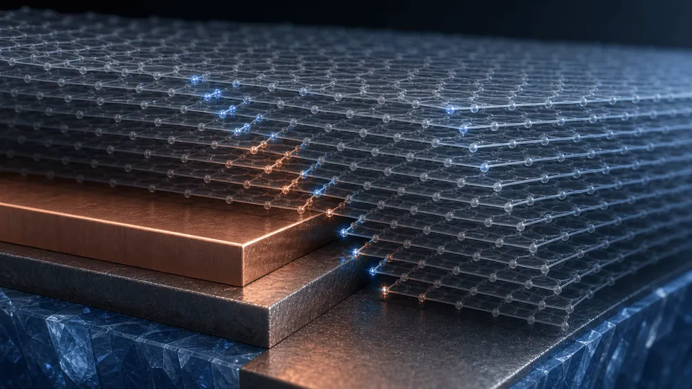
A research team centered at Peking University has grown rhombohedral graphene, in which atomic layers stack in the ABCABC sequence, achieving over 99% phase purity. The resulting regions reach up to 160×80µm, with thicknesses ranging from about 15 layers to roughly 120nm. This advance moves a material that had previously been sought out as rare flakes from exfoliated samples toward deliberate growth on stepped substrates. However, what was made is not a quantum chip. What has shifted here is the possibility of transferring a high-purity stacking phase, needed to study quantum phenomena, into a reproducible growth process.
99% Refers to Stacking-Phase Purity, Not Chemical Purity
The results were published as a peer-reviewed research article in Science on July 23, 2026, by Mengze Zhao, Zhibin Zhang, Xin Sui, and 19 authors in total. The paper is titled "Step geometry–guided growth of rhombohedral graphene," appearing in volume 393, issue 6809, pages 422–427, DOI 10.1126/science.aed9202. Participants included Peking University along with Suzhou Laboratory, ShanghaiTech University, Wuhan University, and the Institute of Physics, Chinese Academy of Sciences.
The paper's "phase purity > 99%" does not mean the carbon in the sample is 99% chemically pure. It refers to the phase purity of the targeted rhombohedral ABC stacking among the graphene layers. Nor is it a measurement of elemental impurity concentration. Shortening this to "99% pure graphene" would misrepresent the nature of the achievement.
The samples reported in the paper measure up to 160×80µm in-plane, with thicknesses ranging from about 15 layers to roughly 120nm. The team also compiled data referencing Raman spectroscopy fingerprints and characteristic band structures, from few-layer films up to bulk samples of about 200 layers. Data released by the authors on Zenodo also includes Raman indices comparing ABC and AB stacking at 4–10 layers and 200 layers. However, the abstract and the published CSV do not indicate the total number of samples or the number of repetitions per condition. The figure of over 99% cannot be read as a production-line yield.
Steps Select for ABC Stacking Order
In typical Bernal stacking, graphene layers stack in the ABAB sequence. In rhombohedral stacking, each layer shifts slightly in the same direction, returning to its original position every three layers in an ABCABC pattern. This difference amounts to nothing more than a lateral shift of a single atomic layer, yet it substantially alters the low-energy electronic states. In few-layer graphene with ABC stacking, flat electronic bands as well as superconductivity, magnetism, and the quantum anomalous Hall effect have each been reported in separate experiments.
The difficulty has been that ABC stacking is thermodynamically metastable and prone to transforming into the more stable AB stacking through interlayer sliding. In an interview with the South China Morning Post, Zhibin Zhang explained that with conventional mechanical exfoliation, the probability of finding the desired stacking was less than 1%. This figure reflects the rate at which exfoliated flakes were found, and is not a before-and-after comparison measured against the same population as the phase purity reported here. It cannot be treated as an effect size of "improvement from 1% to 99%."
The team covered a sapphire surface with fine steps using copper-nickel, guiding interlayer sliding and orientation during growth through the step geometry. The experimentally confirmed results are the area and thickness of the ABC phase grown there, along with its Raman spectra, band structure, and electron transport. In Figure 2J of the authors' published data, the rhombohedral phase fraction was 0.991 with a standard deviation of 0.008 under the condition of angle θ=0°. A correlation was recorded showing this dropping to 0.838±0.121 at 5° and 0.773±0.238 at 10°. However, the published CSV does not include the physical definition of θ or the number of repetitions for each condition. This correlation cannot be regarded as a causal rule holding across all substrates.
Calculations were also used to explain the mechanism. The published data compares the bending energy as layers cross the step at angles φ=75°, 80°, and 85°, while a separate calculation tracks energy changes on a picosecond timescale. These are simulation results supporting the interpretation that step geometry selects for interlayer sliding, not experimental measurements directly capturing phase purity or transport properties. Since the full set of conditions used in the model, such as atom count and temperature, is not included in the published CSV, it would be premature to treat these calculated values as optimal conditions for mass production.
How 160×80µm Changes the Supply of Experimental Material
The maximum size of 160×80µm remains far from wafer scale. Even so, compared to experiments that search flake by flake for the desired stacking among exfoliated pieces, it becomes far easier to plan and secure regions for spectroscopic measurement and electrode fabrication. A 2025 paper in Physical Review Applied reported infrared imaging as a technique for rapidly distinguishing ABC from ABA stacking. The growth method reported here, by contrast, intervenes not at the sorting stage but at the stage of creating the target phase itself.
The value of the grown samples does not end with structural observation. The paper reports layer antiferromagnetism and the quantum anomalous Hall effect based on electron transport measurements. The published data includes transverse and longitudinal resistance from sweeps of a perpendicular magnetic field between −150 and +150mT, along with measurement series including −6 to +6T. These are experimental results. However, since the CSV alone cannot establish the measurement temperature or the total number of devices, it is not possible to determine from the published figures over what temperature range, or in how many devices, the phenomenon was reproduced.
Superconductivity in rhombohedral graphene was reported in 2021, and the quantized anomalous Hall effect in 2025, each in separate peer-reviewed Nature papers. This paper does not represent the first discovery of these phenomena. What is new is that, using high phase purity and larger-than-previous grown samples, the team has prepared a reference material that connects structure, band properties, and transport in a single system. This does not mean that thick grown samples automatically exhibit the same performance as past few-layer devices.
Production Conditions to Verify Before Quantum Chips
Separating what has been confirmed here from what remains unverified clarifies the scope of this research.
| Item | Confirmed in this study | Not yet confirmed |
|---|---|---|
| Material | Over 99% phase purity of ABC stacking | 99% chemical purity representing elemental impurities |
| Dimensions | Up to 160×80µm, roughly 15 layers to 120nm | Continuous wafer-scale film |
| Physical properties | Electron transport measurements of layer antiferromagnetism and quantum anomalous Hall effect | Qubits, gate fidelity, error rates |
| Reproducibility | One peer-reviewed paper and author-published data | Independent replication by another team |
This breakdown also clarifies the distance to quantum computing. No qubits were encoded using this sample, and no quantum gates were operated. Application to quantum chips is a research goal built upon the observed physical properties, not a result directly demonstrated by this experiment.
The next step is to expand the area. It will be necessary to measure whether ABC stacking becomes disordered at boundaries when smaller pieces are joined, whether phase purity is maintained after transfer from the growth substrate, and whether the same transport phenomena appear after electrodes and insulating layers are added. Only about 17 days have passed between the paper's publication and August 9, 2026, so independent replication cannot yet be confirmed. Whether the maximum dimension of 160×80µm can be called a mass-production technology will need to be judged based on the number of samples across multiple batches, uniformity within the area, and device yield after processing.