


Every time the name Rapidus comes up, plenty of people find it hard to understand why a company with no mass-production track record is receiving such enormous sums of taxpayer money. And indeed, Rapidus has never once run a semiconductor mass-production line, yet it is attempting to reach the same cutting-edge 2-nanometer generation as TSMC, Samsung, and Intel. Against the ¥7.3 billion that eight private companies contributed purely as equity, the government's planned total support — combining equity investment and R&D funding — comes to ¥2.9 trillion, a gap of 397 times. What underpins this asymmetric bet are three workarounds that substitute for the missing foundation of mass-production experience itself: importing technology from IBM and others, adopting a production method different from TSMC's, and pouring in funding on a national scale.
¥7.3 Billion From 8 Companies vs. ¥2.9 Trillion From the Government: The Stakes Piled Onto a Company With Zero Mass-Production Experience

At the factory completed in Chitose, Hokkaido, a semiconductor mass-production line has never once been operated. Rapidus Corporation was established on August 10, 2022, with seven companies — Toyota Motor, Sony Group, NTT, SoftBank, NEC, Denso, and Kioxia — each contributing ¥1 billion, and Mitsubishi UFJ Bank contributing ¥300 million. Total investment came to just ¥7.3 billion. On November 11 of the same year, the Ministry of Economy, Trade and Industry (METI) announced, alongside the establishment of the research organization LSTC (Leading-edge Semiconductor Technology Center), that it had selected Rapidus as the domestic manufacturing base for advanced chips. Tetsuro Higashi, former president of Tokyo Electron, became chairman, and Atsuyoshi Koike, a former SanDisk executive, became president.
Seven of the eight investing companies are firms for which stable access to semiconductors is directly tied to their competitiveness. Toyota and Denso have demand for advanced chips in autonomous driving and electrification; SoftBank and NTT have demand tied to data centers. Sony Group represents image sensors, and Kioxia represents memory — both lined up as chip users. Mitsubishi UFJ Bank, a financial institution, joined this lineup from the funding side.
Against this ¥7.3 billion in private investment, the government has laid out a plan to invest a combined ¥2.9 trillion in R&D support and equity by fiscal 2027. A simple comparison shows a gap of several hundred times, and tracing the flow of investment and R&D support makes the exact multiple and breakdown clear. The figures continue to be updated even now.
What Rapidus is aiming for is mass production at the cutting-edge 2-nanometer generation — a level TSMC, Samsung, and Intel have spent decades building up to. The target timeline is set for the second half of fiscal 2027. The combination of a company with no mass-production experience suddenly attempting the world's most advanced process represents the biggest bet in Japan's semiconductor policy.
Mass-producing semiconductors means something different from completing a single prototype. It refers to the repetitive work of continuously firing off thousands, tens of thousands of chips of the same design, gathering data on how defects appear and how variation occurs between machines, and steadily raising the yield. TSMC and Samsung have accumulated this repetition over decades, across millions of wafers.
Rapidus has none of this accumulated experience. Because this repetitive process requires massive capital investment and long years, it is effectively impossible for a latecomer to catch up by following the same path. That is precisely why the foundation of mass-production experience itself must be replaced by other means.
From 50.3% of the World Market to 7%: 36 Years Shaped by US-Japan Friction and a Missed Shift to Horizontal Division of Labor
According to Cabinet Office materials, Japan's semiconductor industry peaked in 1988 with a 50.3% share of the global market — an era in which Japanese companies produced more than half of all semiconductors made in the world. METI materials put the share at 7% as of 2024. The decline from the peak amounts to 43.3 percentage points.
The trigger for the fall was US-Japan friction. On June 14, 1985, the Semiconductor Industry Association (SIA) filed a complaint under Section 301 of the Trade Act, citing barriers to entry in the Japanese market. On June 24 of the same month, Micron Technology separately filed a dumping complaint against Japanese-made DRAM with the USTR (Office of the United States Trade Representative). These led to the signing of the US-Japan Semiconductor Agreement on September 2, 1986. The agreement called for expanding the share of foreign-made semiconductors in the Japanese market and exporting at fair prices, placing constraints on the expansion strategies of Japanese manufacturers.
Around the same time as the agreement, the very formula for winning in the industry began to change. While Japanese companies continued to cling to a vertically integrated model that handled everything from design to manufacturing in-house, TSMC, founded in 1987, put forward a horizontal division-of-labor model — the foundry — that handled only manufacturing. This let design companies avoid owning factories, while TSMC could spread its fixed costs by consolidating orders from multiple customers into mass production. Japan's comprehensive electronics makers prioritized production capacity for their own products, and fell behind in this shift toward division of labor.
The limits of vertical integration were symbolized by Elpida Memory, formed in 1999 by merging the DRAM businesses of NEC and Hitachi. Backed by the government, it was the sole major domestic DRAM specialist and reached third place globally in market share, but filed for corporate reorganization on February 27, 2012. Its debt of roughly ¥448 billion was the largest bankruptcy in manufacturing history at the time, and the company was acquired by Micron the following year.
Vertical integration was not a mistake from the start. In the DRAM market of the 1980s, having a single company handle everything from design to manufacturing and quality control made it easier to stabilize yield and quality, and this was a strength of Japanese manufacturers. The turning point came once semiconductor applications expanded from general-purpose memory toward logic-centric use, and horizontal division of labor — better suited to handling diverse designs — began to gain the advantage in investment efficiency. Japanese companies kept prioritizing their own production capacity through this turning point, and ceded the initiative to dedicated foundries like TSMC.
Not Competing on TSMC's Turf: Rebuilding the Production Method Around Single-Wafer Processing
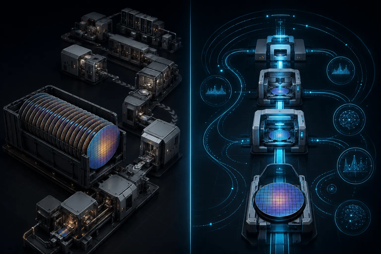
"We can create a different field and market from TSMC." So states Atsuyoshi Koike, president and CEO of Rapidus. Unable to compete on mass-production track record, the company chose to avoid being measured on the same yardstick, and instead decided to rebuild the production method itself.
That production method is a scheme called RUMS (Rapid and Unified Manufacturing Service). It integrates design, front-end, and back-end processes under a single company, end to end, and gathers individual data through an "all-single-wafer process" that handles wafers one at a time. The collected data is analyzed by AI, controlling the process while improving yield.
At conventional foundries like TSMC, the industry standard is to group wafers into "lots" of 25 and transport and manage them as a unit. While single-wafer processing at individual tools — such as exposure or film deposition — is not unusual, the transport between processes and the progress management itself are carried out on a lot basis. Lot-based management suits the efficiency of mass production, but if an abnormality occurs in one lot, a loss across all 25 wafers can occur at once.
RUMS, as Rapidus presents it, replaces this very unit of transport and management with a single wafer, placing at the core of its design philosophy a system that links and analyzes individual measurement data for each wafer throughout the entire process. Conventional foundries are also said to be advancing data collection through AI-based tool and process control, but Rapidus explains that it can identify problematic processes or tools more quickly, making it better suited to responding to demand for diverse, small-batch orders and short delivery times.
Rapidus reportedly aims to cut front-end turnaround time to less than half that of conventional foundries. Even without an accumulated mass-production track record, if the company can win customers through speed from order to delivery, it can avoid the disadvantage of being compared against TSMC on the same terms. This reversal in thinking underlies the rebuilding of the playing field that RUMS represents.
Importing the Missing Experience From Outside: Mobilizing Technology From IBM, imec, and ASML
In December 2022, Rapidus signed a strategic partnership with IBM for joint development of 2-nanometer node technology. Under the agreement, Rapidus engineers are working alongside IBM researchers on joint development of 2-nanometer node technology at the Albany NanoTech Complex in New York State, which is owned and operated by NY CREATES. With no foundation of mass-production experience, the company first chose the path of transplanting technology from a partner with existing know-how.
IBM itself, the party teaching this technology, does not currently operate its own factory mass-producing 2-nanometer generation chips. IBM transferred its semiconductor manufacturing business to GlobalFoundries in 2015, and the Albany NanoTech Complex, where Rapidus engineers absorb technology, is a research and development site, not a mass-production line. What Rapidus is transplanting is not process know-how forged through mass production, but the research-stage technology itself.
Rapidus did not limit its source of technology transfer to IBM alone. On April 4, 2023, it joined the "Core Partner Program" of imec, the Belgian research institute known for its research into EUV (extreme ultraviolet) lithography technology, gaining access to advanced technology, a 300mm pilot line, and constituent technologies for the 2-nanometer generation. On December 14, 2024, the latest EUV lithography machine from the Dutch company ASML, the "TWINSCAN NXE:3800E," arrived at New Chitose Airport, and delivery to the Chitose factory began on the 18th of the same month. This marked the first time a mass-production-grade EUV lithography machine had begun operating domestically.
EUV lithography machines are indispensable for the 2-nanometer generation because the miniaturization needed to shrink circuit line widths to a few nanometers requires resolution only achievable with extreme ultraviolet light. Only one manufacturer in the world, ASML, can produce these machines in volume, and the waiting period for delivery is said to be long. That Rapidus achieved delivery as early as the end of 2024 is one example of compensating for its lack of mass-production experience by prioritizing equipment procurement.
This setup produced its first result on July 18, 2025. Just three months after the Chitose production building IIM-1 went into full operation, Rapidus announced Japan's first confirmed operation of a 2-nanometer generation GAA (Gate-All-Around, a structure in which the gate surrounds the entire channel) transistor. It was a prototype-stage result, not mass production, but this structure is easier to suppress leakage current in than the conventional FinFET (Fin Field-Effect Transistor), though it involves more process steps — making yield optimization the biggest technical hurdle of the 2-nanometer generation. Suppressing leakage current allows higher computing performance at the same power consumption, which especially benefits high-performance chips such as AI accelerators for data centers. Atsuyoshi Koike stated, "We have cleared a major milestone toward mass production in 2027."
On the computing resource side, collaboration with NVIDIA is also being explored. According to the company's Tim Costa, the lithography-focused library "cuLitho" speeds up the generation of OPC (Optical Proximity Correction) patterns — essential for transferring circuit patterns onto photomasks — by 70 times through GPU computation compared to conventional methods, and TSMC has already been using it in mass production since 2024. Another library, "cuDSS," solves linear equations related to physical phenomena at high speed, and verification with TSMC, Samsung Electronics, and EDA giant Cadence Design Systems reportedly showed a 60- to 80-fold increase in the computational speed of finding optimal solutions. Both of these are track records at existing major foundries such as TSMC, and collaboration between NVIDIA and Rapidus remains at an exploratory stage. For a company with no mass-production experience, being able to leverage such external computing infrastructure in the future could become a means of compensating for lack of experience through computing power, by increasing the number of trial-and-error cycles.
Tracing the ¥2.9 Trillion Breakdown: ¥250 Billion in Equity From IPA and ¥631.5 Billion in Commissioned R&D

Government funding flows into Rapidus mainly through two channels. One is equity investment by the Information-technology Promotion Agency (IPA), an independent administrative agency; the other is commissioned R&D from METI and NEDO (New Energy and Industrial Technology Development Organization). IPA added ¥100 billion on February 27, 2026, and another ¥150 billion on June 5, bringing its cumulative investment to ¥250 billion.
Through this investment, IPA holds only 11.5% of voting rights, but it possesses a golden share carrying veto power. A golden share is a type of stock that, regardless of the holding ratio, allows its holder to exercise a veto over specific resolutions concerning the core of management — a mechanism sometimes adopted when the state involves itself in the management of critical infrastructure companies. In Rapidus's case too, the design allows the government to check shifts in mass-production policy or capital strategy without requiring a majority of voting rights. Even with a small share of voting rights, it can control only the decisive moments, letting the government retain the reins of oversight without deeply intervening in day-to-day management. In the same February 2026 period, 32 private companies also made an additional combined investment of ¥167.6 billion, expanding the base of investors well beyond the original eight companies' ¥7.3 billion.
On the commissioned R&D side, METI, through NEDO's Post-5G Fund R&D commissioning program, decided on April 11, 2026, to provide an additional ¥631.5 billion for fiscal 2026. Combined, the government's equity investment and R&D support are planned to reach a total of ¥2.9 trillion by fiscal 2027. Compared to the original ¥7.3 billion pooled by the eight founding companies, this scale is equivalent to 397 times as much. Behind the government's willingness to commit funding at this scale lies an economic security objective: building a system that does not depend on overseas supply for advanced semiconductors. It has also been reported that total investment, including private capital spending, is expected to grow from an initially projected ¥5 trillion scale to around ¥7 trillion.
However, the ¥2.9 trillion figure is only the planned total through fiscal 2027, and the amount actually finalized as of June 2026 is smaller than this. Reports vary, but the amount already decided is estimated to be in the range of roughly ¥2.3 trillion to ¥2.6 trillion. This gap between the plan and the actual results shows that Rapidus's fundraising is still only halfway complete.
IBM, which receives compensation for its technology transfer, domestic manufacturers who can preferentially supply parts and equipment, and the 32 companies that deepened their relationship with Rapidus through investment, are the parties who stand to benefit from this structure. On the other hand, if mass production does not proceed as planned, IPA, as an investor, will incur valuation losses, the cost of which will ultimately be borne by taxpayers. The parties who stand to gain and those who bear the risk of loss are, in this way, clearly separated.
Where the Second Half of Fiscal 2027 Stands as TSMC, Samsung, and Intel Race Ahead
TSMC, Samsung, and Intel are all advancing the rollout of 2-nanometer generation GAA processes between 2025 and 2026. Rapidus's targeted start of mass production is the second half of fiscal 2027 — a start several years behind these three companies. In addition to the gap in mass-production experience, the gap in time also weighs heavily on Rapidus.
EE Times Japan reports that METI has projected that, by fiscal 2030, supply will fall short of global demand for 2-nanometer generation logic semiconductors by 10% to 30%. Even if the market itself has room to grow, whether Rapidus can raise the quality of its mass production to the same level as its competitors is a separate question. Lucy Chen, vice president at Taiwanese research firm Isaiah Research, has commented: "They can manufacture, but there are still doubts about whether they can achieve a level of yield and productivity that generates profit."
Material that counters this skepticism is beginning to gather in the form of customers still at the prototype stage. Fujitsu is moving toward commissioning Rapidus to manufacture a 1.4-nanometer generation NPU (Neural Processing Unit, a computing device specialized for AI processing), with NEDO subsidizing two-thirds of the roughly ¥58 billion development cost. In March 2026, Canon and Synopsys Japan commissioned a prototype of a 2-nanometer generation image processing chip — the first such commission by a major domestic company. On November 17, 2023, Rapidus also reached an agreement with Canada's Tenstorrent on IP development, and is advancing joint development of an AI edge chip based on the 2-nanometer generation. Even without a track record on mass-production lines, RUMS's characteristic of accommodating diverse, small-batch orders and providing individualized support at the prototype stage is drawing in customers.
Lucy Chen's concern also points to the need to separate technical feasibility from business profitability. While all-single-wafer processing is well suited to individualized handling, the number of wafers processed per machine is lower than with lot processing, meaning that securing the same production volume requires investing that much more in equipment and personnel. A change of just one percentage point in yield significantly shifts the number of good chips obtainable from a single wafer, and if mass production continues with low yield, the manufacturing cost per unit will end up higher than competitors'. The high fixed-cost structure that comes with RUMS's strength in diverse, small-batch production is also a factor increasing Rapidus's reliance on government funding.
Land Prices in Chitose Rose 44.1% in a Year — the Bet Is Already Moving the Local Economy
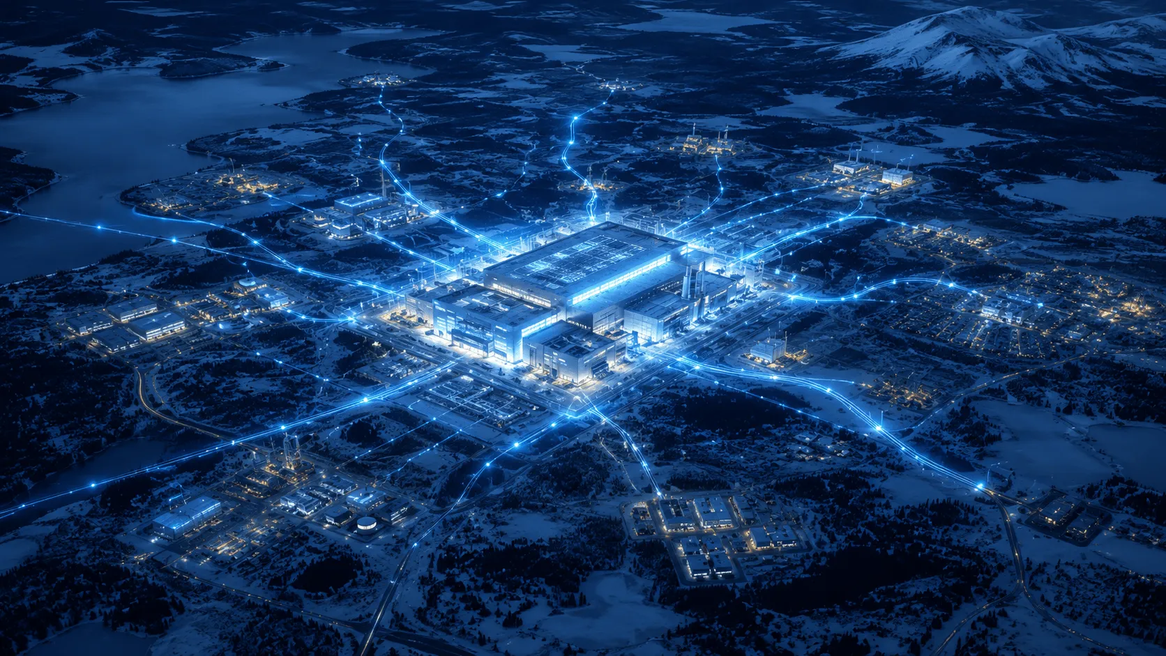
In the official land price announcement published by the Ministry of Land, Infrastructure, Transport and Tourism as of January 1, 2026, the area around JR Chitose Station in Chitose City rose 44.1% year-on-year, the highest rate of increase in the country. Citywide average land prices rose 11.85%, and commercial land alone rose 29.67%, reaching roughly triple the level seen in 2022. Whether Rapidus's mass production succeeds or fails will not be known until fiscal 2027 or later, but land prices are already moving as if pricing in that outcome in advance.
The reason a semiconductor factory's arrival pushes up land prices is that demand for relocation among related companies and employees emerges ahead of the start of mass production itself. Suppliers of materials and equipment, as well as partner companies handling construction and maintenance, are gathering around the Chitose factory, and housing demand for employees and their families is also swelling. Hokkaido has put forward the "Hokkaido Valley" initiative, aiming to turn the belt stretching from Chitose through Ishikari to Tomakomai into a hub for advanced technology, and related investment is spreading, including SoftBank's announcement that it will build a data center using renewable energy in Tomakomai.
In November 2023, the Hokkaido New Industry Creation Organization (ANIC) estimated the economic ripple effect on the premise that Rapidus begins mass production in fiscal 2027, projecting a cumulative maximum of ¥18.8 trillion through fiscal 2036. Even under a scenario in which only the first-phase Chitose factory (IIM-1) is built, the ripple effect across all of Hokkaido is projected to reach a cumulative ¥10.1 trillion over 14 years, boosting the region's gross domestic product (GDP) by ¥6.1 trillion. The 44.1% rise in land prices is an already-realized measured value, while the ¥18.8 trillion figure is an expected value that will only materialize if Rapidus succeeds in mass production. The market, in other words, has priced in the outcome before the success or failure of mass production is even known.
According to a survey published in May 2025 by Frog Inc., which aggregates job listing site data, the minimum monthly salary listed in job advertisements within Chitose City rose 46.42% over two years, the highest growth rate in the country. This local sense of exhilaration — with both land prices and wages climbing — stands in contrast to the trajectory of Elpida Memory in the past. Elpida's 2012 bankruptcy is reported to have imposed a burden of roughly ¥28 billion on taxpayers, a past example showing that investment in state-led semiconductor projects does not always bring benefits to the region or the public.
The Second Half of Fiscal 2027 Will Put Zero Mass-Production Experience to the Test
What Rapidus has built up since its founding in August 2022 are three workarounds: external mobilization of technology borrowed from IBM, imec, and ASML; RUMS, a production method different from TSMC's; and ¥2.9 trillion in funding. It was a bet that, even without mass-production experience itself in hand, combining these three could fill in the missing foundation. The confirmed operation of a 2-nanometer GAA transistor in July 2025 shows that this bet has cleared its first technical hurdle.
If mass production cannot begin in the second half of fiscal 2027, the operating cash flow break-even targeted for fiscal 2029 will not materialize, and the free cash flow break-even and stock listing targeted for fiscal 2031 beyond that will also slip further away. In this sense, the roadmap Rapidus has laid out is a single connected line. Conversely, once the first hurdle of beginning mass production is cleared, the remaining two financial targets move into a stage where they can be verified with concrete numbers: mass-production yield and order volume.
Given the fall from 50.3% in 1988 to 7% in 2024, and the two defeats represented by that decline and Elpida's 2012 collapse, METI chose not to further support existing companies but instead to establish a new one. The reasoning behind establishing a new company rather than supporting existing ones has been explained only in limited terms by those involved, but it can be read as a formation designed not to repeat the past failure of clinging to vertical integration and self-reliance. In this sense, Rapidus represents Japan's semiconductor industry's second national experiment.
As the second half of fiscal 2027 approaches, the indicators to watch narrow down. Will the Chitose factory's yield be disclosed? Will prototype-stage customers such as Fujitsu and Canon commit to mass-production orders? And how will the remainder of the government's planned ¥2.9 trillion be disbursed? The outcome of this bet — attempting the cutting edge with zero mass-production experience — will reveal itself once these three figures come together.