


When people talk about semiconductor miniaturization, attention tends to focus on how fine a line EUV lithography can draw. But if the material can't be etched exactly as drawn, that line is meaningless. Reactive ion etching (RIE), the dominant dry-etching method, removes substrate material using highly chemically reactive plasma — a process that has long carried side effects such as substrate damage, redeposition of etched debris, and rising costs. Sanghyun Lee, HyunWook Ra, and Keun Hee Bai of Samsung Electronics have published a paper in the Journal of Vacuum Science & Technology A (JVST A) discussing the industrial application of atomic layer etching (ALE), an alternative approach to this problem. AIP's official announcement (Scilight, dated August 28, 2026) quotes Bai as saying the technology can create "a uniform width and a 90-degree angle" in layers.
Why Etching Has Become Semiconductor's Weak Point
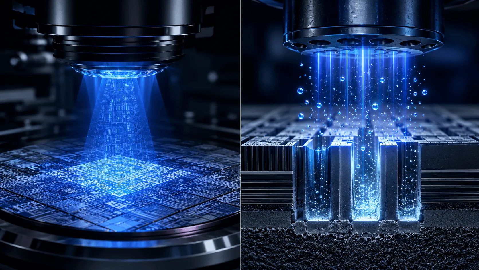
RIE's weakness emerges as a trade-off for its speed and versatility. The method removes material by bombarding the substrate with ions in a plasma — fast, but prone to damaging areas beyond the intended target, and prone to redeposition, where removed material resettles on the chip surface. Now that fine wiring widths have shrunk to the nanometer scale, this side effect has become directly tied to production yield. Over the past several generations, improvements in semiconductor performance have largely been framed around how fine a line EUV can expose, while the limitations on the processing side — how precisely the drawn line can actually be etched out of the material — have received comparatively little attention.
RIE also requires costly equipment and consumables, and depending on the material being processed, selectivity (the ability to etch only the intended layer while leaving others intact) can be insufficient. This weakness becomes especially pronounced with fragile materials such as low-k materials (low-dielectric-constant insulating materials used to suppress parasitic capacitance, crosstalk, and signal delay between interconnects). No matter how fine a pattern EUV can draw, the chip won't come out as designed unless the material can be etched to match. The etching process has long been treated as an unglamorous supporting player, but it is increasingly becoming one of the main battlegrounds for pushing the limits of miniaturization.
How ALE Removes Material One Atomic Layer at a Time
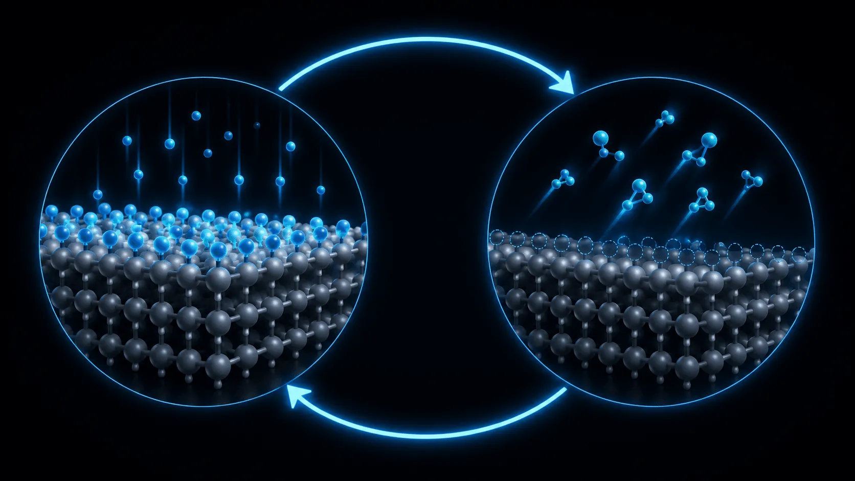
The decisive difference between ALE and RIE is that ALE doesn't remove material all at once; instead, it alternates between two steps — surface modification and selective removal. Ideally, a reactive gas or plasma first chemically alters (or thinly deposits onto) only the outermost surface of the substrate, and then a separate step using low-energy ions or a different reaction selectively removes just that modified layer. Because the reaction doesn't readily reach the unmodified material beneath, the thickness removed per cycle tends to stay within a few atomic layers. This near-"self-limiting" property is considered the reason ALE can achieve lower damage and higher selectivity than RIE. However, in actual processes like the fluorocarbon-based ALE discussed in this paper, this ideal self-limiting behavior doesn't hold perfectly — it's known to exhibit more complex behavior, where the amount of deposition varies depending on processing time and the pattern's aspect ratio.
In AIP's announcement, Bai states: "Many studies have pointed to ALE's advantages of low damage, high selectivity, and precise control, but we add to that the advantage of a more vertical profile — ALE's ability to create a uniform width and a 90-degree angle in layers." According to the paper, this verticality is achieved by actively exploiting the property whereby deposition behavior changes depending on pattern shape. Whereas in RIE, the etch rate and angle are influenced by plasma conditions and sidewalls tend to tilt or widths tend to vary, this kind of control allows ALE to more uniformly produce nearly vertical walls along the depth direction. This precision is exactly why ALE has drawn attention in advanced processes that need to preserve fine interconnect spacing.
At the same time, this approach comes with a trade-off. Because the amount removed per cycle is small, more cycles are needed to etch the same depth, and the equipment configuration tends to become more complex. This is why conventional ALE has carried the drawbacks of low throughput and complex processing. While RIE controls the amount removed by time, ALE determines it through the self-limiting nature of the chemical reaction. This difference in design philosophy — prioritizing precision over speed — is what separates the strengths and weaknesses of the two approaches.
The Barrier and Progress Revealed in Samsung's Paper
The paper, titled "Current status of atomic layer etching and its adoption to low-k fine patterning: An industrial perspective," was published in JVST A, Volume 44, Issue 5, as article number 058501 (DOI: 10.1116/6.0005592). The authors are Sanghyun Lee, HyunWook Ra, and Keun Hee Bai, and AIP introduced the content in a Scilight article dated August 28, 2026. According to the paper, Samsung has applied ALE in two processes on its logic and DRAM mass-production lines since 2017, and added a third application process in 2021. ALE itself is already an established mass-production technology at Samsung; what this paper focuses on is the challenge of extending that track record into a new application area — the fine processing of low-k materials.
Regarding the O2-based ALE used for fine processing of low-k materials, the paper reports that profile control (the precision of the etched shape) has improved through reduced ion-induced damage, but chemical damage caused by oxygen radicals and the resulting degradation of dielectric constant (capacitance degradation) remain unresolved. It cannot yet be said that low damage and high verticality have been achieved simultaneously, and new challenges remain that differ from the existing application areas with a proven mass-production track record. Specific reduction rates or target process nodes are not disclosed in the published material. That said, the research team suggests that many of the challenges around throughput, particles, and stability could be resolved through careful process design optimization and architectural simplification, while addressing the chemical damage caused by oxygen radicals would require optimizing material conditions and shifting to O2-free chemistries. Regarding this extension into low-k materials, the paper has not reached the stage of declaring mass-production readiness or a breakthrough.
Notably, Bai and colleagues have also published an earlier paper (JVST A, Vol. 43, Issue 6, 062603) addressing vertical trench control for high-density low-k materials. This latest paper builds on that earlier work, stepping back from individual experimental results to reframe the discussion around how ALE might be adopted by industry more broadly. Since the two papers address different subjects, they should be read as distinct works rather than conflated.
The Comeback of a Once-Abandoned Technology
The concept of ALE itself is not new. According to a technology history review published in JVST A, the earliest identifiable report dates back to 1988, when Yoder applied the approach to diamond film processing. Later research has also revealed that a patent forming the prototype of ALE was filed by Iwamatsu in 1981. In the 1990s, it was proposed as a sequential, self-limiting process alternating between surface modification and removal, but at the time it was dismissed as too slow, and it never became a mainstream mass-production technology.
This trajectory parallels the path taken by ALD (atomic layer deposition), another atomic-layer-scale process. ALD, too, was initially shunned for its slow film-formation speed, but as miniaturization progressed and thin-film uniformity became a critical mass-production issue, its precision came to be valued, and it became established as an industry-standard technology. A similar dynamic appears to be at work behind ALE's renewed attention in the 2020s: as the dimensions being processed shrink, the relative value of a technology that etches precisely — even if somewhat slowly — increases.
This broadening reappraisal is also reflected in market estimates. According to a forecast from a single market research firm (GM Insights), the ALE equipment market is expected to grow from $1.2 billion in 2025 to $2.5 billion by 2034, with Lam Research holding a 31.4% share and Applied Materials 29.5% as the top two companies as of 2024. The same estimate puts the top five companies — including Tokyo Electron (19.6%), Oxford Instruments (3.1%), and SAMCO (1.7%) — at 85.3% of the total equipment market. Converting at ¥159.38 to $1 (as of August 27, 2026), $1.2 billion is roughly ¥191.3 billion, and $2.5 billion is roughly ¥398.5 billion.
However, these figures remain small relative to the industry as a whole. A forecast from a different research firm (Precedence Research) projects that the overall semiconductor etching equipment market will grow to $56.1 billion (roughly ¥8.9 trillion) by the same year, 2034. Since the sources differ, a direct comparison isn't valid, but in terms of order of magnitude, the ALE market ($2.5 billion) accounts for less than 5% of that figure — suggesting it remains a niche segment within the broader etching equipment market.
SAMCO's Early Commercialization, and the Barrier Still Ahead of Samsung
ALE's commercialization has already moved beyond the theoretical stage and reached the market in some areas. On December 17, 2025, Kyoto-based SAMCO announced the full-scale sale of ALE systems for GaN/SiC processing: the 4-inch research system "RIE-400iP-ALE" and the 8-inch mass-production system "RIE-800iPC-ALE." GaN (gallium nitride) and SiC (silicon carbide) are materials used in power semiconductors, a field with growing demand for electric vehicles and industrial equipment.
However, while SAMCO's equipment and the target of Samsung's paper are both ALE, their applications differ. SAMCO's systems are focused on GaN/SiC processing for power semiconductors, whereas the ALE that Samsung has been running in mass production since 2017 for logic and DRAM, and the low-k material processing for interconnect layers discussed in this latest paper, involve different target materials and different precision requirements. It's more accurate to understand the area where the Japanese company has commercialized production equipment, and the area where Samsung has built up a track record on its own production lines, as separate applications of the same underlying technology lineage. For Samsung, extending into low-k materials looks like a case of putting a technology with an established production track record up against a new kind of barrier.
What Samsung's paper does not say is also clear. It doesn't reveal when the low-k application will move into mass production, how the chemical damage and capacitance degradation caused by oxygen radicals will be resolved, what specific process nodes are being targeted, or how competing foundries such as TSMC will respond. The path the research team has outlined — resolving many of the remaining challenges through careful process design, optimization, and architectural simplification — is the concrete work that will next be tested to see whether it can fill in these blanks.