

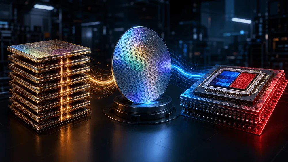
Samsung Electronics and Broadcom have signed a memorandum of understanding (MOU) projecting their collaboration spanning memory and foundry at over $200 billion over five years through 2030. The signing took place on July 24, 2026, at the AI Summit held in San Francisco. The scope is broad, covering everything from HBM supply to sub-2nm manufacturing and 2.3D/2.5D packaging. However, the $200 billion figure has not been announced as a confirmed order value. What's new here is that memory, logic, and packaging—the components that make up AI accelerators—have been brought under a single collaborative framework.
What "Over $200 Billion" Represents
Samsung's announcement estimates the scale of the collaboration the two companies are pursuing in memory and foundry at over $200 billion over the five years through 2030. The announcement takes the form of an MOU, and it does not state that Broadcom has already placed orders for that amount, nor that Samsung has secured it as revenue. Figures broken down by product area and minimum purchase amounts have not been disclosed, and unit prices and volumes remain unknown.
This distinction cannot be dismissed as a mere footnote to the headline. While the five-year estimate reportedly includes HBM supply and contract manufacturing of Broadcom products, Samsung's English-language announcement describes the scope of the figure as "memory and foundry." The Korean-language announcement emphasizes the collaboration as a whole, including advanced packaging, but does not indicate the contractual breakdown. Therefore, the $200 billion figure cannot be equated with foundry-only orders or currently guaranteed revenue.
At the same time, this doesn't mean the number is hollow. The two companies are expanding their existing business relationship into a long-term development and supply framework for next-generation AI infrastructure. The practical weight of this MOU lies in establishing a relationship through 2030 in which Samsung can propose memory and manufacturing processes simultaneously for Broadcom's next-generation products.
Bundling HBM and 2nm Into the Same Development Plan
In memory, Samsung is pursuing collaboration to supply HBM for Broadcom's next-generation AI accelerators. In foundry, the plan calls for using Samsung's sub-2nm processes for Broadcom's Wireless Broadband Communications (WBC) products, among others. Broadcom's customer names and accelerator product names have not been disclosed.
Broadcom's AI semiconductor business offers numbers that explain why it needs to lock in supply arrangements early. In its fiscal 2026 second quarter, the company's AI semiconductor revenue reached $10.8 billion, up 143% year-over-year. For the third quarter, it expects $16 billion, an increase of over 200% year-over-year. Custom AI accelerators and AI networking are driving this growth. Compute chips alone don't make a finished product—HBM and advanced manufacturing need to be secured on the same timeline.
Samsung, for its part, already has the manufacturing foundation in place to begin this collaboration. The company began mass shipments of HBM4 in February 2026, and on May 29 announced sample shipments of 12-layer HBM4E. Mass production of HBM4E will begin after sample evaluation and optimization are completed, in line with customer schedules. In foundry, Samsung began mass production of first-generation 2nm products in Q4 2025 and has laid out plans to launch second-generation 2nm mobile products in Q2 2026. This MOU is not a pledge tied to an unfinished roadmap—it's a framework linking technologies that have already moved to mass production or customer evaluation with Broadcom's product plans.
2.3D and 2.5D Bridge Memory and Logic
Advanced packaging is the process that brings HBM and 2nm manufacturing together into a single AI semiconductor. Samsung has named 2.3D and 2.5D packaging technologies built on its 2nm process as part of the collaboration. Placing miniaturized logic and HBM close together to widen inter-chip bandwidth while keeping power consumption and heat generation in check requires packaging design to be worked out in parallel with the manufacturing process.
2.5D Cube-S places logic and HBM horizontally on a silicon interposer, creating high-bandwidth, low-latency connections. Within 2.3D, there are two variants: Cube-E, which embeds a silicon bridge capable of fine wiring into an RDL interposer, and Cube-R, which uses an organic RDL interposer. Samsung describes Cube-E as offering cost efficiency when scaled up in size, and Cube-R as an option that is easier and cheaper to scale up.
In other words, 2.3D and 2.5D are not simply different names for the same packaging method. Depending on the bandwidth, footprint, and cost Broadcom requires, the interposer structure can be chosen accordingly. If Samsung can handle memory, 2nm logic manufacturing, and packaging all together, it may be able to reduce the design coordination needed across departments and external companies. Samsung says it aims to shorten development timelines by connecting co-optimized design and process all the way through to mass production.
Three Conditions to Verify Before the Dollar Figure
The process by which this MOU moves toward actual supply can be tracked through three conditions. The first is the allocation between memory and foundry, which are explicitly named as the target of the over-$200-billion figure. Once a breakdown is released, it will become easier to judge how much revenue will actually flow into each of Samsung's two businesses. Advanced packaging is included in the scope of collaboration, but the announcement does not specify it as part of the $200 billion allocation. Commercial terms such as pricing and volume need to be verified separately.
The second is the timing of customer evaluation and mass production. HBM4E remains at the sample stage, and the tape-out, qualification, and mass production start date for the 2nm chip intended for Broadcom products have not been disclosed. Samsung's Q1 2026 earnings materials indicated an outlook for advanced-node production lines to reach full utilization in the second half of the year, but the volume allocated to Broadcom remains unknown.
The third is whether ordering conditions such as minimum purchase volumes will be disclosed, and whether individual supply contracts can be confirmed. This announcement does not reveal cancellation terms, and exclusivity or production sites have not been indicated either. Until these are disclosed, the over-$200-billion figure cannot be treated as an upper limit or a guaranteed amount for the collaboration—it must be read as the scale the two companies project over five years. The next milestone will not be a restatement of the dollar figure. It will be whether HBM qualification, mass production of 2nm products, and concrete ordering conditions come together within the same product plan.