

Samsung Electronics' HBM4 yield has reached nearly 80%, Seoul Economic Daily reported on August 9, 2026. The figure was said to be under 60% when mass production began in February, meaning the company reached its original year-end target roughly four months early. Samsung has officially announced mass production and shipments to customers, but has not disclosed yield figures. Still, if this improvement holds across the entire production line, it would speed up the conversion of the already-announced sales to NVIDIA and the supply collaboration with AMD into shipment volume and revenue.
From under 60% to nearly 80% in six months
According to industry sources cited by Seoul Economic Daily, the yield rose from under 60% at the start of mass production to nearly 80% over roughly six months. The publication describes the 80% range as a "golden yield" benchmark that signals stable production and improved profitability. Having approached its year-end target as of August, Samsung is said to be in a position to accelerate the expansion of HBM4 supply.
What can be confirmed from official announcements is that mass production has already progressed to product shipments. On February 12, Samsung announced it had begun mass production of HBM4 and shipped commercial products to customers. Its Q2 earnings materials also explicitly noted expanding HBM4 sales and stated that the first samples of HBM4E had been sent to major customers. However, the language Samsung uses in its own materials goes only as far as "stable yield"—the specific figures of 60% and 80% come from Seoul Economic Daily's reporting.
Yield refers to the proportion of manufactured chips or packages that can be shipped as good units. Assuming the same input volume, improving from 60% to 80% increases the number of shippable units and lowers the manufacturing cost borne by each good unit. In a phase where HBM is in short supply, this difference affects both the volume that can be delivered to customers and profitability. Samsung itself, in its Q2 earnings materials, projected that even with increased production, demand for server DRAM, enterprise SSDs, and HBM would continue to outpace supply.
Why yield matters for 12-layer HBM4
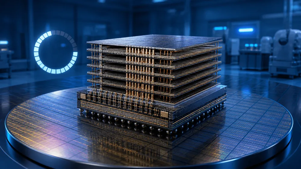
Samsung's mass-produced product stacks DRAM dies in 12 layers, with a logic base die controlling signals and power placed beneath them. It uses a 6th-generation 10nm-class "1c" process for the DRAM and a 4nm process for the base die. Because the process spans memory fabrication, logic fabrication, and stacked packaging, an increase in defects at any stage reduces the yield of finished products. The reported 80% yield figure draws attention because it suggests Samsung may be nearing a level where it can stably produce, at mass-production scale, 12-layer products that combine these advanced processes.
The product's performance specifications are already public. It stably achieves a per-pin transfer speed of 11.7Gbps, which can be pushed up to a maximum of 13Gbps. This is about 46% higher than the 8Gbps standard value Samsung cites for HBM4, and per-stack bandwidth reaches up to 3.3TB/s. The capacity of the 12-layer product ranges from 24GB to 36GB, with plans to expand to 48GB in a future 16-layer version.
With HBM4, the number of data I/O pins doubled from HBM3E's 1,024 to 2,048. More wiring makes it harder to design signal paths while suppressing power consumption and heat. Samsung states that through low-voltage TSVs and optimization of the power delivery network, it improved power efficiency by 40% compared to HBM3E, reduced thermal resistance by 10%, and improved heat dissipation performance by 30%. Whether Samsung can keep increasing the number of good units that pass performance tests at the specified speed is the condition for converting the spec sheet's performance into actual supply capacity.
Customer adoption is settled—next comes volume
Samsung and AMD signed a memorandum of understanding in March covering HBM4 supply for the Instinct MI455X, among other collaborations. According to AMD's official specifications, the MI455X is equipped with 432GB of HBM4, with a theoretical maximum memory bandwidth of 23.3TB/s. Mass production deployment of Helios, which incorporates 72 MI455X units, is expected to begin in the second half of 2026. In its Q1 earnings, Samsung stated it had also begun mass-production sales of HBM4 for NVIDIA's Vera Rubin.
With these customer deals in place, the value of improved yield translates directly into sales plans. According to Seoul Economic Daily, Kim Jaejune, the executive vice president who leads Samsung's memory business, said at the Q2 earnings call that Q3 HBM4 sales would more than triple from the previous quarter, and that HBM4's share of total HBM sales would exceed 60% in the second half of 2026. If a yield near 80% can be sustained, it would support this sales growth from the production side.
However, a rise in yield is not the same as a rise in market share. Memory for AI accelerators only advances to mass-production shipment after passing speed and power-consumption tests and receiving certification from each individual customer. Supply volume depends not only on the number of good units but also on production capacity, customer-specific allocation, and product mix. A single figure of 80% cannot by itself tell us whether the gap with SK hynix has closed, or whether allocation to NVIDIA has increased.
What to check after the "80%" figure
The report does not clarify which process stage serves as the denominator for the 80% yield figure. The meaning of the number changes depending on whether it refers to DRAM wafers, good dies, packages after stacking, or final inspection. The capacity and speed grade covered, the production line, and the inspection conditions also remain unknown. Comparing this figure with other companies' yields would require values measured under the same process and conditions.
The same caution applies to the next-generation HBM4E. On May 29, Samsung officially announced sample shipments of its 12-layer, 48GB product. It achieves stable operation at 14Gbps with a maximum of 16Gbps, and bandwidth of up to 3.6TB/s per stack, with mass production timing to be aligned with customer schedules. Seoul Economic Daily reported that the reliability-test yield had risen above 70%, but Samsung has not disclosed this figure itself, and it cannot be directly compared with the 80% figure reported for HBM4 mass production.
Whether Samsung's HBM4 has truly advanced in the mass-production race will become clear based on whether it can more than triple Q3 sales and maintain its good-unit rate after increasing output. As for HBM4E, once customer certification is complete and the mass-production timeline is finalized, it will be possible to judge whether the manufacturing process built up around HBM4 has been successfully carried over to the next-generation product.