


Samsung Foundry has officially announced it will delay the mass production target for its cutting-edge 1.4nm process by two years, from the original 2027 to 2029. This can be seen as the beginning of a painful yet significant strategic shift that bets on the company's future—one that temporarily steps back from the long-standing "node supremacy" race with TSMC in favor of prioritizing near-term profitability and business stabilization. How will this bold pivot affect the balance of power in the semiconductor industry, particularly the competitive dynamics with TSMC?
The Announced "Two-Year Delay" - A Difficult Decision Prioritizing Practicality Over Pride
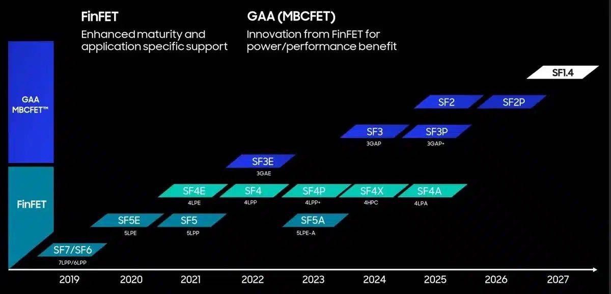
This policy shift was revealed at the "SAFE (Samsung Advanced Foundry Ecosystem) Forum 2025," an event for partner companies held in Seoul, South Korea on July 1, 2025. According to reports from Korean media outlet ETNews and others, Samsung executives presented an updated roadmap that explicitly listed the introduction of the 1.4nm process as 2029.
This represents a significant setback from the ambitious "2027 mass production start" target announced in 2022. More importantly, TSMC—Samsung's biggest rival—plans to begin mass production of its 1.4nm-equivalent process, "A14," in 2028. This makes it all but certain that Samsung will fall at least a year behind TSMC in bringing the most advanced node to market.
For Samsung, a company that has long fought a fierce battle over the title of technological "world first," voluntarily disclosing this delay speaks to an extremely weighty management decision—one that prioritizes business reality over pride.
"Why" the Delay? - A Double Bind of Massive Losses and Low Yields
No single factor drove Samsung to this historic strategic shift. Rather, a serious financial situation and technical challenges have become intertwined in a complex way.
Worsening Financial Conditions and the Reality of Customer Attrition
The biggest reason is the deteriorating profitability of the foundry business. According to multiple reports, Samsung Foundry is estimated to have posted a massive operating loss of approximately 4 trillion won (roughly 420 billion yen) last year. The company had fallen into a structure where enormous R&D expenses and capital investment for cutting-edge processes were squeezing profits.
Some sources have also previously pointed to another factor behind the delay: "key customers that had expressed interest in the 1.4nm process have walked away." Even if you develop a technically world-leading process, without major clients willing to adopt it, you cannot recoup your investment, and factory utilization rates won't rise. This harsh business reality likely delivered the decisive blow that forced a reconsideration of the 1.4nm plan.
The Deep-Rooted Yield Problem - The Price of the "World First" Title
In 2022, Samsung began mass production of its 3nm process featuring GAA (Gate-All-Around) transistor structure—a "world first" ahead of TSMC—and showcased its technological prowess to the world. However, it was something of an open secret in the industry that behind the scenes, the company was struggling with severely low yield rates.
Yield rate—the proportion of good chips obtained from a single wafer—is a lifeline directly tied to manufacturing cost and supply capacity. If this figure remains low, a company cannot supply customers with stable quality and quantity, and it loses their trust. Previous reports have indicated that Samsung had targeted a 70% yield rate for its 3nm GAA process but failed to achieve it.
Recent reports suggest that the yield rate for the next-generation 2nm process has improved to around 40% (Japanese), but this still falls short of TSMC's reported level of over 60% for the same process. It's not hard to imagine that this experience led to today's cautious approach, which prioritizes technological maturity over the risk of a premature launch.
"Profit" Over "World First" - Samsung's New Survival Strategy
This decision is not merely defensive. It marks a turning point toward a new survival strategy aimed at more realistic and sustainable growth.
Concentrating Resources on 2nm and Monetizing Existing Processes
Samsung is temporarily shifting its focus away from 1.4nm and concentrating its resources on perfecting the 2nm process. According to the roadmap, the company plans to refine it through a second generation (SF2P) and a third generation (SF2X) by 2028, thoroughly sharpening its competitiveness at the 2nm node. There are also reports that major companies like NVIDIA have shown interest in Samsung's 2nm process, and if Samsung can make this process a success, it could serve as a major foothold for business recovery.
At the same time, the company is also focusing on improving utilization rates for processes that are several generations old but still in high market demand—such as 4nm, 5nm, and 8nm—to reliably generate profit. This can be described as an extremely rational strategy: by stepping back from the cutting-edge race, Samsung aims to maximize the use of its existing strengths and assets to improve its financial standing.
What Breaking Away from "Node Supremacy" Means
This series of moves signals Samsung's departure from the "node supremacy" mindset it has long clung to—the idea that leading rivals in the miniaturization race is the ultimate imperative.
The company once went head-to-head with TSMC, staking its pride as the "Samsung of technology." But it has now confronted the harsh reality that this competition did not necessarily translate into business success. This should perhaps be viewed as a "strategic retreat"—acknowledging short-term defeat in order to lay the groundwork for long-term victory. Catch your breath, solidify your footing, and wait for a reliable opportunity to counterattack. That is Samsung's new game plan.
The Dawn of a TSMC Monopoly? Impact on the Semiconductor Industry
Samsung's strategic shift has the potential to significantly redraw the balance of power in the semiconductor industry.
TSMC's Established Dominance in Leading-Edge Processes
With TSMC set to begin mass production of 1.4nm (A14) in 2028, its leadership in cutting-edge technology will likely remain unshaken for at least the next few years. Top-tier companies pursuing maximum performance—such as Apple, NVIDIA, and Qualcomm—are expected to become even more dependent on TSMC. TSMC's dominant position in the foundry market may become even more entrenched.
What Comeback Scenarios Remain for Samsung
Still, it would be premature to conclude that the outcome has already been decided. Samsung still has scenarios available for a comeback.
The key lies, once again, in GAA technology. If Samsung can fully unlock the potential of GAA transistors—which theoretically offer superior power efficiency and performance compared to conventional FinFET structures—in its 2nm process, the situation could change. If Samsung can reliably supply products that surpass TSMC's 2nm process (expected to be the final generation of FinFET technology) in performance or cost, it is not impossible to win back customers who once walked away.
This decision can also be understood not as Samsung's declaration of defeat at 1.4nm, but as a strategic move to designate "2nm GAA" as the main battleground and secure a decisive victory there. Over the next few years, it will be worth watching closely how Samsung Foundry rebuilds its business and improves profitability under this new strategy, and what changes this brings to the global semiconductor supply chain. Samsung's challenge—shifting from chasing the cutting edge to a more strategic and realistic business model—will surely be an important development in forecasting the future of the semiconductor industry.
Sources