

In 1995, William Wulf and Sally McKee of the University of Virginia sounded an alarm in a short paper. Processor performance was growing exponentially, but DRAM bandwidth could only grow at a far slower pace. The gap would keep widening, they warned, until computers became mere memory-waiting machines. They named this problem the "Memory Wall."
Thirty years later, that warning has become reality. Over the past 20 years, the peak computing performance of server-grade AI hardware has grown 60,000-fold, while DRAM bandwidth has grown only 100-fold and interconnect bandwidth only 30-fold. The computational demands of training large language models (LLMs) are expanding at a pace of 750x every two years, and simply keeping compute units fed with data has become the single biggest obstacle to AI scaling.
The semiconductor industry's answer to this wall, deployed since 2013, has been High Bandwidth Memory (HBM). Jointly developed by AMD and SK hynix, it was adopted as an industry standard by JEDEC in October 2013. DRAM dies are stacked vertically using TSVs (Through-Silicon Vias) and connected to the processor through an ultra-wide 1024-bit interface. Starting from 128 GB/s in the first generation of HBM, bandwidth reached 2 TB/s per stack with HBM4, whose specification was finalized in 2025. That amounts to roughly a 16-fold increase in bandwidth over 12 years.
However, HBM has carried a structural constraint since its inception that has never changed. The memory stack sits "beside" the processor, and data travels horizontally across the silicon interposer. This horizontal distance has set the ceiling on both bandwidth and power efficiency.
From "side-by-side" to "stacked on top": how the Z-axis changes the data path
On August 4, 2026 (local time), at the keynote of Future of Memory and Storage (FMS) 2026 held in Santa Clara, California, Samsung Electronics unveiled the industry's first concept model that overturns this horizontal arrangement entirely: a new concept called "zHBM (Z-axis High Bandwidth Memory)." The "z" in the name refers to the vertical direction—the Z-axis.
Kim Kyungryun, Senior Vice President and project leader of the DRAM design team, described the limits of existing packaging structures in the keynote: "With existing packaging structures, there is a limit to how close we can bring the accelerator chip and the memory physically. By introducing GAA (Gate-All-Around) transistors into HBM for the first time and applying a 2nm foundry process, we overcome this wall."
VP Kim also closed the keynote by declaring, "Samsung is back." This is a statement of confidence following a bitter period in 2024 when Samsung fell behind in HBM3E quality verification for NVIDIA and lost leadership of the AI memory market to SK hynix—before achieving the industry's first HBM4 mass shipments in February 2026.
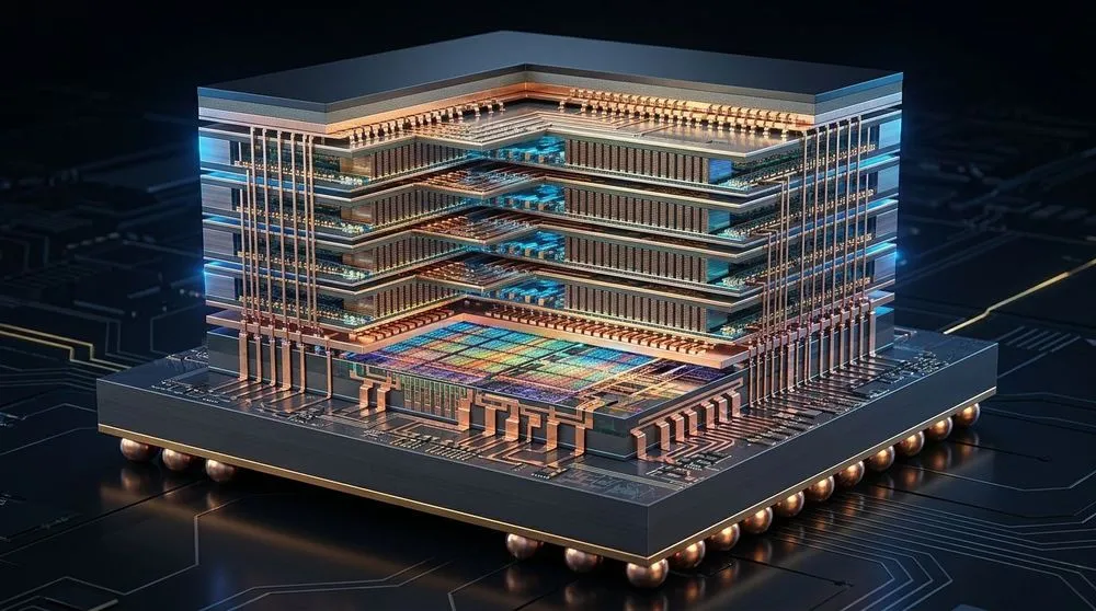
The structure of zHBM is simple and clear. Rather than laying the HBM stack horizontally on the interposer, it is stacked vertically directly on top of the AI accelerator die. The physical distance data must travel is shortened, simultaneously reducing signal propagation delay and power loss.
How to read the multipliers: the figures Samsung presented and their premises
The numerical targets for zHBM that Samsung announced in its official newsroom are presented in comparison with HBM5. However, this comparison requires some context.
As of August 2026, JEDEC has not yet finalized the specification for HBM5, and commercialization is expected around 2028. Therefore, the claim of "8x over HBM5" is not a comparison against a finalized specification, but a calculation based on Samsung's own internal design targets for HBM5.
Looking at Samsung's published bandwidth targets by HBM generation: for HBM4, the JEDEC specification of 2 TB/s per stack (2048-bit interface, pin speed of roughly 8 Gbps) has already been finalized. For HBM5, Samsung's FMS 2026 roadmap sets a target of expanding the interface width to 4096 bits, achieving approximately 4 TB/s per stack. Stack capacity is expected to grow from HBM4's maximum of 48 GB to 64 GB or more, but Samsung has not yet disclosed detailed specifications for HBM5 (pin speed, power consumption, stack height, etc.).
Using this "assumed HBM5" as the baseline, the figures Samsung claims for zHBM are summarized below.
| Metric | HBM5 (Samsung's internal assumption) | zHBM (Samsung's claim) | Multiplier | Notes |
|---|---|---|---|---|
| Memory bandwidth per GPU | ~4 TB/s (assumed) | ~32 TB/s equivalent | ~8x | Calculation based on Samsung's design target, since HBM5's specification is not yet finalized |
| Memory density per GPU | Unpublished | 10x or more | >10x | Vertical stacking is expected to reduce interposer area, allowing more stacks within the same footprint |
| Energy efficiency (power per bit) | Unpublished | 3x | 3x | Explained as mainly due to reduced signal power from shorter wiring length |
| Thermal resistance | Unpublished | Reduced by 50% or more | ~0.5x | Assumes application of the HPB (Heat Path Block) structure |
Care should be taken with the phrase "per GPU" in the table. This does not refer to bandwidth per stack, but to the total bandwidth of all memory connected to a single AI accelerator (GPU). With zHBM, vertical stacking increases the number of stacks that can be placed within the same footprint, causing the total bandwidth per GPU to surge.
All of these figures are Samsung's design targets, not measured values. Since the actual performance of HBM5 itself—the baseline for comparison—has not been finalized either, the validity of these multipliers cannot currently be verified externally.
Hybrid copper bonding and GAA: the three technical pillars supporting zHBM
The technology that makes zHBM possible rests on three pillars.
First, hybrid copper bonding. Conventional HBM bonds dies together using microbumps (solder protrusions), but hybrid bonding joins copper directly to copper. Eliminating the need for bumps dramatically reduces the gap between dies, raising signal transmission speed. According to a report by the Korea Times, Samsung combined hybrid copper bonding with multi-wafer bonding to increase signal transmission speed while also lowering thermal resistance.
Second, the first-ever introduction of GAA transistors into HBM. GAA is a structure in which the gate surrounds all four sides of the channel, giving it higher current control than planar or FinFET structures. By combining this with a 2nm foundry process, Samsung aims to give HBM's base die more logic performance than ever before, blurring the boundary between memory and processor.
Third, a heat dissipation structure called HPB (Heat Path Block). According to a report by the Seoul Economic Daily, Samsung applied a new heat dissipation structure technology to the sides of the core die, lowering thermal resistance by 50% or more compared to HBM5. This is a design philosophy that addresses the intuitive concern that stacking memory on top of the processor would make heat harder to escape, by providing a dedicated heat path.
Rivals counter with "cooling": a comparison with SK hynix's iHBM
While zHBM tackles the problem through a "shift in placement," rival SK hynix is approaching the same wall through "innovation in cooling." In May 2026, SK hynix announced its HBM5-oriented technology, "iHBM." It embeds a highly thermally conductive silicon component called ICE (Integrated Cooling Element) inside the package, directing heat away directly from the D2D PHY area, where heat concentrates most. The reduction in thermal resistance is reported to be 30% or more compared to conventional designs.
| Item | Samsung zHBM | SK hynix iHBM |
|---|---|---|
| Approach | Vertically stacks memory on top of the processor | Embeds a cooling element inside the package |
| Thermal resistance reduction | 50% or more compared to HBM5 | 30% or more compared to conventional |
| Target generation | HBM5 and beyond (concept stage) | HBM5 (mass production expected 2029–2030) |
| Maturity | Concept / mockup | Verification stage as a packaging technology |
| Customer compatibility | Supports insertion of an intermediate layer for custom IP | Design-compatible with existing SiP environments |
The two companies are tackling the same problem (the trade-off between heat and bandwidth) along different axes, and NVIDIA is reportedly evaluating both technologies at this stage. Which one is ultimately adopted will likely depend on mass-production yield and system integration efficiency.
Micron, too, shows no sign of easing its pursuit. Its HBM production capacity for 2026 is already fully sold out, and it has raised its forecast for the HBM market size to $100 billion by 2028—two years earlier than its previous projection. Micron plans to introduce HBM4E in 2027.
The basis for "Samsung is back," and the IDM strength behind it
Behind Samsung's ability to present zHBM as a concept lies the fact that it is the only IDM (Integrated Device Manufacturer) in the world that holds memory, foundry, and advanced packaging capabilities all under one roof. For HBM4 mass production (February 2026), Samsung combined a 1c DRAM process with a 4nm logic base die. While rival SK hynix prioritized stability by using the previous-generation 1b process, Samsung claims to have adopted the most advanced node from the outset and achieved stable yield without redesign.
As of Q1 2026, Samsung held a 38.5% share of the DRAM market and a 31.6% share of the NAND flash market, ranking first in the world in both (according to TrendForce). The zHBM concept can be read as an attempt to extend this vertical-integration capability into next-generation architecture.
At the same FMS 2026 event, alongside zHBM, Samsung also showcased zNAND-O (next-generation NAND for edge AI) and the V10 BV-NAND with over 400 layers (achieving a 58% improvement in memory density over the previous generation through wafer bonding). Around 30 memory and storage technologies were on display in total, with zHBM positioned as one "vision" among them.
Beyond 2028: uncertainties remaining before mass production
Samsung has not indicated a concrete timeline for the commercialization of zHBM. With HBM5 mass production expected around 2028, zHBM's introduction would come after that. Considering that SK hynix's HBM5 is projected for 2029–2030, the entire industry is currently in a transitional period, searching for what comes "after HBM."
Not a few challenges remain. In a structure where memory is stacked on top of the processor, the escape route for heat is structurally constrained. While the HPB approach has been proposed to address this, its thermal behavior in real hardware remains unverified. Mass-production yield for hybrid copper bonding is also still at the verification stage across the industry as a whole. Counterpoint Research has analyzed that full-scale adoption of hybrid bonding will not come until the HBM5 generation or later.
Furthermore, the "8x performance" claimed for zHBM is per-GPU performance, and how much this contributes to overall system performance improvement will depend on the accelerator's design and workload. While the design flexibility of inserting an intermediate layer for custom IP is appealing, it remains unclear how much optimization cost this will impose on each customer.
The "wall" that Wulf and McKee described in 1995 is still standing, even thirty years later. zHBM is an attempt to break through that wall along the Z-axis, and if realized, it would mark the first turning point in HBM's 12-year evolutionary history where the very principle of placement changes. For now, however, it remains at the stage of mockups and numerical targets. Whether the wall truly comes down will have to wait for the day this concept is implemented in silicon.