

Today's semiconductor memory, the backbone of digital computing, has achieved reliable computation by strictly maintaining binary logic—zero and one. This all-or-nothing mechanism, which clearly distinguishes between the presence or absence of charge stored in a capacitor, or between a transistor's on and off states, delivers high reliability for deterministic program execution. However, in the fields of neuromorphic computing, which mimics the structure of nervous systems, and edge processing, which extracts features directly near sensors, this strict binary nature demands a heavy price instead. Every time continuous analog signals are converted into discrete bit strings and shuttled back and forth between memory and processing units, enormous amounts of power and time are lost.
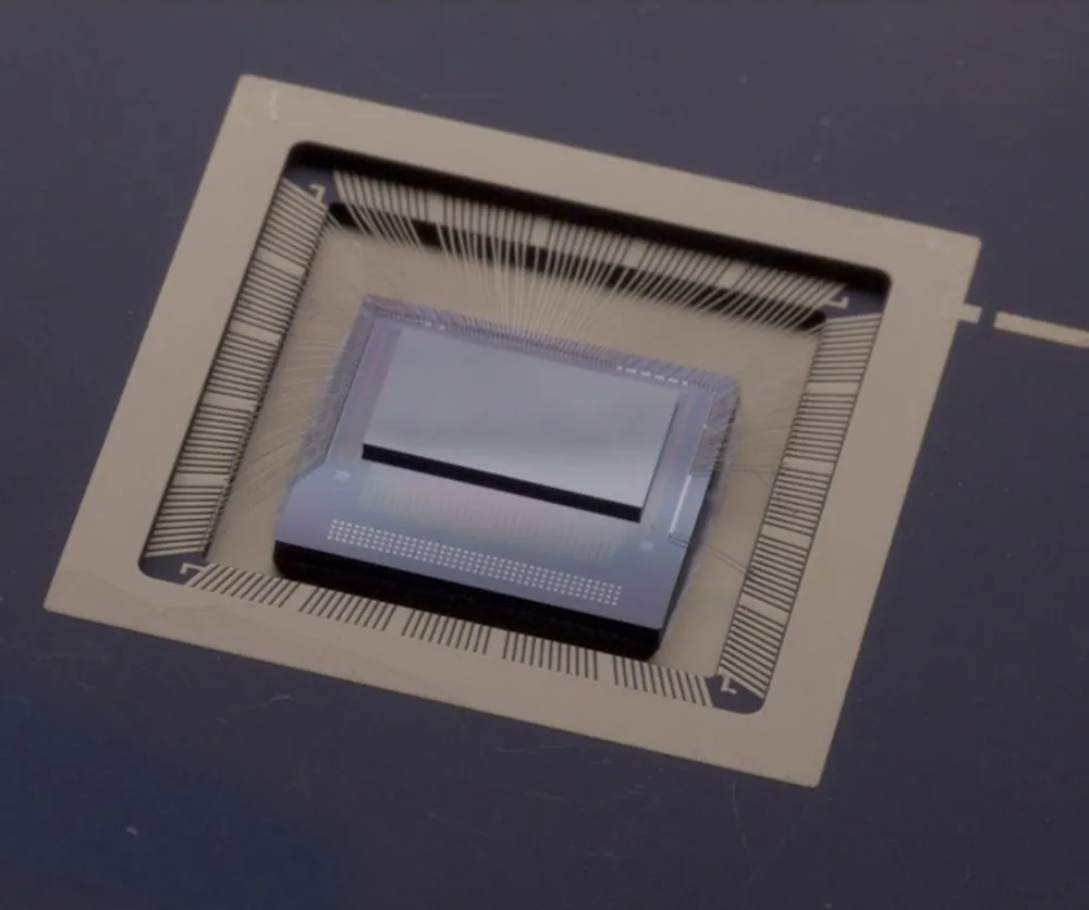
A research team at Sandia National Laboratories has reported a new memory device that tackles this constraint from the standpoint of materials physics. By combining electrochemical phase control in a vanadium oxide thin film with localized thermal excitation, the team succeeded in eliciting both smooth, synapse-like resistance changes and nonlinear, neuron-like switching behavior from a single microscale device. The findings were published in the peer-reviewed journal Science Advances on July 10, 2026 (DOI: 10.1126/sciadv.aee1908). However, this achievement represents a functional demonstration of a single component in a laboratory setting—it is neither a commercialized memory product nor a technology ready for immediate market deployment. To separate excessive expectations from established facts, this article examines the physical mechanisms and performance boundaries in detail.
Between the Peer-Reviewed Paper and the Press Release: What Sandia's Single Device Actually Demonstrated
The original research paper was authored by a team led by Elliot Fuller and Alec Talin of Sandia National Laboratories, with Sangheon Oh serving as first author. The paper is titled "Multifunctional electrochemical memory stabilized by phase coexistence," with co-authors including Adam L. Gross, Adam S. Christensen, Jacklyn Zhu, Patrick S. Finnegan, Joshua D. Sugar, Sean R. Bishop, Simeon J. Gilbert, R. Stanley Williams, Perla B. Balbuena, Kyung Seok Woo, Timothy D. Brown, and Suhas Kumar.
In science and technology reporting, the point demanding the most careful attention is the gap that can arise between the physical properties directly measured in a peer-reviewed paper and the future application prospects portrayed in a research institution's press materials. In this announcement, the data explicitly presented in the paper is limited to the electrochemical and thermal response characteristics of a single test device fabricated in a laboratory environment.
This device is based on a concept called Electro-Thermo-Chemical RAM (hereafter ETCRAM). While ordinary memory devices are typically built to specialize in a single function—for example, merely retaining a resistance value—the research team focused on electrochemically controlling a phase-coexistence state within a single device to elicit distinct operating modes. This is not a guarantee of operation on a commercial memory product or a large-scale integrated circuit manufacturing line; rather, it represents a stage of basic research in which the underlying physical principle has been demonstrated in the form of a single device.
Electrochemically Locked Phase Coexistence and Local Heating: Two Operating Principles Coexisting in One Device
The core of the ETCRAM published in Science Advances lies in a microstructure that vertically integrates phase-separated vanadium oxide () used in both the channel and reservoir layers. Conventional electrochemical memory (ECRAM) works by moving ionic species such as lithium or oxygen ions through an electrolyte, injecting or extracting ions from the lattice of a host material to continuously change electrical conductivity. However, when attempting to speed up ion migration at room temperature, the written state tends to be lost easily, as if through self-discharge. Conversely, if the energy barrier for ion migration is designed to be high in order to enhance non-volatility, then large write voltages or long pulse widths become necessary, causing a marked drop in operating speed—a persistent dilemma.
The research team adopted a structure that dynamically overcomes this kinetic barrier using localized heat. A heater function is integrated into the gate electrode, and a localized electrical pulse is applied only at the moment of writing to generate active heat. Because this heat temporarily lowers the kinetic barrier within the material, ion rearrangement and redox reactions complete rapidly even at low applied voltages. Once heating stops and the device returns to room temperature, the high barrier is restored, and the injected state becomes firmly locked within the material's internal phase-separated structure.
According to the paper's abstract, this single device achieved smooth and stable analog conductance programming, similar to a synapse, through the stabilization of phase coexistence corresponding to different redox states. Vanadium oxide has the property of adopting diverse crystalline phases depending on its oxidation state, and by continuously varying the local phase ratio, intermediate resistance states can be finely controlled. To examine resilience under harsh conditions, this phase-separated vanadium oxide ETCRAM device was placed at a high temperature of 200 °C and subjected to a retention test lasting 10,000 seconds. Conductance loss in the high-conductance state was limited to just 0.09%, while loss in the low-conductance state was contained to 10.3%.
Sandia's Talin used a metaphor in the press release to describe this state-retention mechanism, comparing it to "unplugging a battery from a charger while it's only half charged." Just as a battery retains its charge level even when disconnected midway through charging, this device also maintains its intermediate redox state, which is then read out as a continuous analog value. However, this is an intuitive explanation intended for a general audience and does not represent the raw physical measurement data of the device itself.
データを表で見る
| Conductance Loss Rate After 10,000 Seconds (%) | |
|---|---|
| High-Conductance State (High State) | 0.09 |
| Low-Conductance State (Low State) | 10.3 |
Furthermore, the paper demonstrated that the same single component exhibits neuron-like nonlinear switching by leveraging the thermally driven metal-insulator transition (MIT) of vanadium dioxide (). When an appropriate external electrical load is applied, self-heating within the device triggers a sharp phase transition from the insulating phase to the metallic phase, producing threshold-type sharp switching and spontaneous oscillatory dynamics.
Integrating non-volatile analog resistance change—a synaptic function—together with sharp threshold switching—a neuronal function—within a single microscale device has long been considered an extremely difficult challenge. The authors conclude that electrochemically stabilized phase coexistence "could unlock" such analog electronics, but this is a statement of future possibility, not an assertion that a complete, large-scale functional system has been achieved.
Nine Orders of Magnitude and 3,000 Levels: Specific Figures from Two Different Papers
Sandia's press materials cite extremely impressive numbers regarding ETCRAM's performance. Co-developer Fuller stated in the release that the device achieved "100 times higher precision compared to existing state-of-the-art technology, with at least three orders of magnitude wider dynamic range." However, this comparison is a quote from the researcher himself referring broadly to other analog memory technologies in general; the specific measurement definitions of the compared existing technology and the absolute values for both sides are not disclosed in the public materials. Nor is this an objective benchmark verified through testing by an independent standards body.
A crucial point to untangle when scrutinizing this context is the fact that the press materials, under the umbrella project name "ETCRAM," conflate data from two distinct peer-reviewed papers published around the same time. The multifunctional synapse-and-neuron operation achieved through phase coexistence was demonstrated in the aforementioned Science Advances paper on vanadium oxide, whereas the extremely wide nine-order-of-magnitude resistance range and precise number of levels were demonstrated in a separate paper using tantalum oxide () as the material system.
The tantalum oxide research, led by first author Adam L. Gross, was published in the journal Device (DOI: 10.1016/j.device.2026.101217). In this study, a device was fabricated using tantalum oxide for both the channel and reservoir layers, and yttria-stabilized zirconia (YSZ) as the solid electrolyte, with an electro-thermal gate electrode included. The measured active area was a single device measuring 8 .
| Item | Multifunctional Vanadium Oxide Device (Science Advances) | High-Precision Tantalum Oxide Device (Device) | Earlier Micro Vanadium Oxide Study (PR Materials) |
|---|---|---|---|
| First author, journal | S. Oh et al., Science Advances (2026) | A. L. Gross et al., Device (2026) | S. Oh et al., Phys. Rev. Materials (2025) |
| Material composition | Channel, reservoir: phase-separated | Channel, reservoir: , electrolyte: YSZ | Channel: , solid electrolyte |
| Main demonstrated function | Single-device integration of synapse-like analog memory and neuron-like switching | 9-decade conductance tuning range, over 3,000 programmable states | Filament-free uniform phase coexistence, room-temperature non-volatility |
| Key quantitative figures | 200 °C accelerated test (after 10,000 s): 0.09% loss (high state), 10.3% loss (low state) | Programming voltage under 2 V, write speed as fast as 15 ns, endurance exceeding $10^5$ cycles | Estimated conductance change under 1% over 14 years at room temperature |
| Limitations and challenges | Array-scale operation not demonstrated, need to control uniformity of phase transition | Reducing device-to-device variability, faster operation via thinner electrolyte, need for oxygen-diffusion-blocking layer | No thermal electrode integrated, so neuron-type threshold switching not included |
The specific measurement figures reported in the Device paper are striking. The programming voltage was kept below 2 V, and resistance-state updates were confirmed using electrical pulses as fast as 15 ns (nanoseconds). The tunable range of analog conductance reached nine orders of magnitude ($10^9$-fold), within which more than 3,000 distinct states could be identified and written. Note that regarding this nine-decade dynamic range, the paper's abstract presents only the ratio of the tunable range; the absolute upper and lower bound values of measured conductance are not disclosed in the public materials. The linearity of the current-voltage (I-V) characteristics was maintained over a range of six orders of magnitude. Additionally, a rigorous encapsulation structure using silicon nitride ($\text{SiN}_x$) was applied to prevent unintended oxygen diffusion from the surrounding atmosphere from altering the composition. Endurance testing recorded more than $10^5$ (100,000) repeated read and write cycles.
As a small-scale integration test, the research team fabricated a 4 4 array structure. When each device in the array was written to a target value across a conductance range spanning five orders of magnitude, the average deviation of devices from the target value stayed within 0.64%. However, as the authors themselves candidly note in the paper, these prototype devices are "far from being perfected." Further noise reduction, improved write speed through thinner electrolyte layers, and improved retention characteristics through material alloying and precise energy-barrier engineering remain essential challenges.
Notably, in a preprint related to this tantalum oxide device (arXiv:2505.15936), the authors state that "matrix-vector multiplication efficiency could exceed 1,000 TOPS/W (1,000 trillion operations per second per watt)." This figure of 1,000 TOPS/W is merely a theoretical prediction based on simulation, not a value obtained from measuring power on an actual assembled circuit.
The Context of Edge Processing Demand: A Power-Saving Hypothesis and the Research Team's Vision
Behind the research team's urgency in developing this technology lies a pressing concern over the explosive increase in power consumption accompanying the rapid spread of artificial intelligence. Sandia's press materials cite an estimate from the U.S. Energy Information Administration (EIA), noting that under a high-demand scenario, annual electricity consumption by data center servers could reach approximately 800 billion kilowatt-hours (kWh) by 2050. This astronomical figure of 800 billion kWh is a long-term future projection based on specific assumptions, not a confirmed current consumption figure.
What the researchers are pursuing is the hypothesis that memory capable of holding numerous stable analog states within a single device could handle certain types of processing using substantially less energy than existing digital computing methods. This power-saving potential, too, remains at this stage a hypothesis undergoing experimental verification—it is not a power-saving achievement proven on an actual working system.
As an application, the research team envisions "edge processing" or "near-sensor processing," in which computation is performed as close as possible to the source of the data—the sensor itself. Postdoctoral researcher Adam Gross points out the reality that countless sensors are embedded in everything around us, from smartphones and alarm clocks to state-of-the-art automobiles.
For example, in a smartphone camera module, if all the raw analog signals captured by the photodetector are converted into high-resolution digital data and transferred to the main processor or a cloud server for processing, power consumption spikes in both the communication path and the circuitry. If a low-power processing circuit using analog memory is placed right next to the sensor to complete initial image screening and feature extraction on the spot, the amount of unnecessary data that needs to be sent to higher-level circuits can be greatly reduced. This usage scenario presented by the research team is a vision indicating a future direction to pursue; it does not mean that a camera module was actually prototyped in this experiment and transfer power reduced.
This research project was conducted with funding from Sandia's "Laboratory Directed Research and Development (LDRD)" program and the U.S. Department of Energy's Office of Science. Additionally, this technology was selected as a finalist for the 2026 "R&D 100 Award," which represents recognition from an evaluating body of the technology's originality, but is distinct from a guarantee of commercial performance or proof of manufacturability at scale. The research team is currently proceeding with tests of new designs employing further variations in material combinations.
The Path from a Single Device to an Integrated System: Verified Facts and Remaining Challenges
To objectively evaluate this research, it is essential to compare it against prior work and to identify and exclude misunderstandings found in some secondary reporting. Sandia's group reported earlier results on a vanadium-oxide-based ECRAM in the journal Physical Review Materials in August 2025 (OSTI ID: 2584903). This earlier study achieved a uniform phase-coexistence state at room temperature without filament formation, demonstrating high non-volatility with conductance loss estimated to stay under 1% over 14 years at room temperature. Synaptic function via voltage application and logic-gate operation were also confirmed.
The advance achieved by the current Science Advances paper lies in vertically miniaturizing and integrating the device structure and further incorporating a local self-heating gate. This addition of thermal control has enabled the sharp, neuron-like threshold switching—something not achievable in earlier devices—to be drawn out within the same device that also exhibits synapse-like analog memory.
Here, readers should be wary of numerical conflation appearing in some secondary media coverage. For example, the technology news site ElectronicsForU and others reported on this ETCRAM using figures such as "95% reduction in required device count," "99.7% reduction in recall time," and a "64 64 memristor array." However, these extremely favorable figures were mistakenly carried over from an entirely unrelated hyperdimensional memristor study published in Nature Communications. Sandia's ETCRAM research results contain no data whatsoever regarding a 64 64 array or a 95% reduction in device count.
The scientific fact currently established is the physical phenomenon itself: that combining electrochemical oxygen-vacancy injection with thermal activation in a micro-scale vanadium oxide thin film produces dual behavior—analog memory and threshold switching—within a single component. Whether this will dramatically reduce the power consumption of conventional AI hardware, however, must await verification as an actual working integrated circuit.
When thousands of devices are packed at high density on a wafer, how will thermal interference from localized self-heating on neighboring devices be prevented? As miniaturization progresses, to what extent will non-uniformity in phase separation increase device-to-device variability? And how will this be reconciled with existing silicon CMOS manufacturing processes? Whether the physical functional elegance of a single device can evolve into a system capable of supporting the harsh computational demands of the real world hinges on future replication and engineering verification of these as-yet-unresolved challenges.