

The ceiling on how much memory can fit onto a single GPU has long been a burden in AI development. The latest MoE (Mixture of Experts) models, with total parameter counts reaching into the trillions, must spread the portions that don't fit onto a single GPU across multiple GPUs—and every time they do, communication latency and cost pile up. Addressing this wall, a new NAND-based memory called "HBF" (High Bandwidth Flash), developed by Sandisk with SK hynix collaborating on standardization and commercialization, has arrived carrying specs of 1.6TB/s read bandwidth and 512GB capacity. As reported by The Register on July 30, 2026, this technology comes with the technical backing to push GPU memory into the terabyte class, while also carrying the precedent of Intel Optane—a proprietary standard that vanished before it could take hold.
Inside the 1.6TB/s, 512GB Spec: How HBF Works
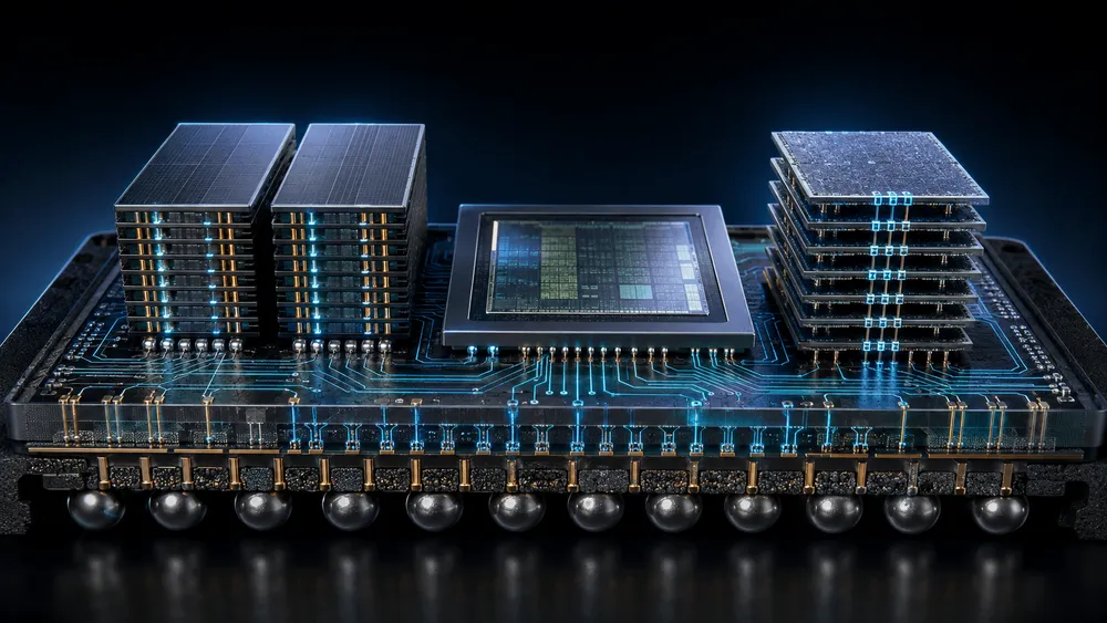
The core of The Register's report is the observation that HBF—a new NAND-based memory standard developed by Sandisk with SK hynix collaborating on standardization and commercialization—has the potential to lift GPU memory from the gigabyte class into the terabyte class. HBF is built on a design based on NAND-type flash memory, and like HBM (High Bandwidth Memory), it shares the trait of stacking dies using through-silicon vias (TSVs). A concept has been presented in which it would be implemented alongside HBM on the interposer of a GPU package, though the specific wiring scheme and packaging method for the upper dies are not yet finalized specifications. The physical mechanism for retaining information is fundamentally different from HBM, which uses DRAM cells.
According to Sandisk's official fact sheet, the first-generation spec stacks 256Gbit/die dies in 16 layers to achieve 512GB of capacity, with read bandwidth reaching 1.6TB/s. This bandwidth is roughly 100 times that of a typical PCIe 5.0-generation NVMe SSD (about 14GB/s), an order-of-magnitude speed for a storage-derived memory. A roadmap has also been published, with plans to expand to over 2TB/s bandwidth and 1TB capacity in the second generation, and 3.2TB/s bandwidth and 1.5TB capacity in the third generation.
Because NAND cells retain information by trapping charge in an insulating film, that film degrades with every write, placing an upper limit on write endurance. Access latency is also longer than DRAM's; The Register's analysis notes that while HBM responds on the order of nanoseconds, HBF's latency remains in the microsecond range. This difference in origin will end up largely dictating HBF's use cases, as discussed below.
What Kimi K3's 2.8 Trillion Parameters Reveal About the Reality Facing GPU Memory
How severe the GPU memory crunch has become is easier to grasp through a concrete model than through abstract argument. Moonshot AI's Kimi K3 has 2.8 trillion total parameters in an MoE configuration with 896 experts, of which only 16 are activated during inference, keeping active parameters at just 104B.
Assuming 2.8 trillion parameters are held at 8-bit quantization, the required capacity comes out to roughly 2.8TB by simple calculation. Bundling six of HBF's first-generation 512GB stacks yields about 3.07TB—enough, in theory, to hold the entire model of this scale. That's a comparable count to the 6-8 HBM stacks typically found in commercial AI accelerators, putting the capacity needed to house an entire model in a single package within reach.
If the same 2.8TB had to be covered using only standard HBM4 (equivalent to 36GB per stack), the required stack count would come to roughly 78 by simple calculation. Even switching to the newer 48GB-equivalent HBM4E would still require about 59 stacks. Given that commercial AI accelerators typically carry around 6-8 HBM stacks, these numbers are far too large to fit within the physical area of an interposer.
Of the 896 experts, only 16 are actually accessed during inference, while the remaining 880 sit idle, unread and unwritten, for most of any given inference step. Writes to the weights stored in HBF occur mainly during model loading or weight updates, and inference execution consists almost entirely of reads. NAND cells have a limit on write cycles, but for the use case of housing expert weights that are rewritten only infrequently, this constraint becomes a relatively light burden. This imbalance is precisely what offsets HBF's weakness. Sandisk EVP and CTO Alper Ilkbahar has stated, "You need large memory bandwidth to feed data to the compute, but you don't have enough memory to fit the whole model on the GPU"—a comment that underscores the need to pair HBM, whose capacity alone falls short, with a large-capacity layer like HBF.
Prefill, the phase where a prompt is read in and context is built, is where weight reads and writes to the KV cache are concentrated. Decode, the phase of generating tokens one at a time, is where read access to the same weights repeats. In a design that assigns infrequently-activated experts to HBF and frequently-accessed layers plus the KV cache to HBM, the write-heavy load of prefill would be handled by HBM, while HBF functions primarily as a large-capacity warehouse for read operations. That said, because the router dynamically selects which experts activate on a per-token basis, it isn't the case that the same fixed 16 experts always reside on the HBM side.
Sandisk has tested the validity of this design philosophy through its own simulations. Reproducing the weight-loading behavior of Llama 3.1 (405B, 8-bit quantized weights) on a GPU performance model, the company claims the performance gap compared to an ideal condition using unlimited-capacity HBM alone came to just 2.2%. The subject of this validation was Llama 3.1, a dense model—not a large-scale MoE model like Kimi K3. And since the test didn't account for the KV cache or real-world operational workloads, it should be read with some caution. Still, it does lend support to the basic design direction of routing infrequently-accessed weights to HBF.
Is the "8-16x versus HBM" Claim Real?
On its own blog, Sandisk claims it can achieve 8-16 times the capacity of HBM at equivalent cost. HBM4 is the standard specification already shipping in volume with a 12-layer stack equivalent to 36GB, while the HBM4E that SK hynix and Samsung are bringing to market is an enhanced sample boosting that to 48GB equivalent. Dividing the 512GB of first-generation HBF by the 36GB capacity of standard HBM4 yields about 14x. Using the 48GB-equivalent HBM4E as the denominator shrinks that to about 10.7x. Given how much the figure shifts depending on which generation is used for comparison, the reality is closer to this: Sandisk's claimed "8-16x" range holds near its upper bound of 14x only when compared against standard HBM4, while comparison against the enhanced HBM4E pushes the number closer to the lower bound.
According to The Register, HBM4 in a 12-layer stack reaches bandwidth of around 2.5TB/s. By contrast, reporting from the semiconductor-focused outlet Mobile MASR indicates that the latest HBM4E mass-production samples from SK hynix and Samsung reach around 3.6-4TB/s, opening a bandwidth gap between generations of as much as 1.5x or more. HBF's 1.6TB/s bandwidth looks unimpressive next to the latest HBM4E, but HBF isn't meant to replace HBM. It's designed as a tier that supplements capacity.
The Ghost of Intel Optane
Intel Optane was a non-volatile memory using phase-change memory (3D XPoint), manufactured in volume by only two companies: Intel and Micron. According to a separate article The Register published on July 29, 2026, what sealed its demise was an awkward price-performance position—consistently more expensive than NAND at the same storage density, yet weaker in performance than DRAM—combined with an inability to keep pace with NAND's bit-density improvement race. In 2021, Micron announced it would end development of 3D XPoint products, pulling out as the sole volume-production partner, and Intel effectively withdrew as well in 2022.
The Register looks back on this outcome as "the KV cache killer that could have eased soaring RAM prices." The lesson Optane left behind is this: a proprietary technology carried by a single vendor or a small handful of vendors struggles to compete on cost against the two dominant camps of NAND and DRAM, which hold the advantage of production scale—and it carries the inherent fragility that a single partner's withdrawal can spell the technology's end outright. Since HBF, too, is a standard led by just two companies, Sandisk and SK hynix, it isn't immune to this same structural risk.
Perhaps mindful of this lesson, the two companies launched a standardization workstream under the Open Compute Project (OCP) in Milpitas, California, on February 25, 2026. SK hynix President and Chief Development Officer Ahn Hyun stated, "The key to AI infrastructure lies not just in the performance race of individual technologies, but in optimizing the entire ecosystem"—a comment that reads as a strategy shaped by learning from Optane's failure as a cautionary example.
Neither Sandisk's nor SK hynix's public materials disclose specific write-cycle endurance figures, pricing, or firm adoption commitments from GPU vendors. There remains a distance between holding a standardization event and actually securing firm adoption commitments from major GPU vendors like NVIDIA and AMD. Technical analysis from Blocks and Files notes that while 768GB with a 12-layer stack and over 1TB with 16 layers are theoretically possible, the growing complexity of interposer wiring counts and TSVs poses a major barrier to mass production. Technical backing and the cost competitiveness underpinned by mass-production scale are separate matters—and this is precisely the boundary where Optane stumbled.
Kioxia's Third Path
Japan's Kioxia is also developing its own High Bandwidth Flash-like technology in parallel. The prototype it announced in August 2025 features specs of 5TB capacity and 64GB/s bandwidth, using a PCIe 6.0-based daisy-chain configuration.
The Sandisk/SK hynix approach achieves bandwidth by stacking dies via TSVs and implementing them directly on the GPU package's interposer. Kioxia's approach connects multiple memory boards and controllers within a module via a daisy chain, linked to the host server by a single PCIe 6.0 x8 connection—a configuration whose bandwidth comes to only about 1/25th of first-generation HBF's 1.6TB/s, but in exchange secures an order-of-magnitude-larger capacity of 5TB in a single module.
The HBF from Sandisk and SK hynix is designed as a high-speed capacity-expansion layer placed right next to the GPU, whereas Kioxia's approach is closer to a large-capacity cold-storage layer positioned one step further out from the GPU's perspective. The two make contrasting trade-offs between bandwidth and capacity. Rather than one replacing the other, they may end up serving distinct roles within the layered structure of an inference system.
Kioxia's project receives support from Japan's NEDO (New Energy and Industrial Technology Development Organization). While the standardization of the specification led by Sandisk and SK hynix proceeds within an international framework, the fact that a Japan-originated technology is building an alternative solution atop the existing industry standard of PCIe illustrates that the contest for leadership in AI memory won't end in a single winner-takes-all outcome.
Two Remaining Hurdles Before Implementation: Standardization and Vendor Adoption
According to Sandisk's public materials, samples of first-generation HBF are planned for release in the second half of 2026, followed by samples of AI inference devices equipped with HBF in early 2027. Industry sources anticipate commercialization arriving between late 2027 and 2028, with full-scale data center demand growth expected around 2030. The period from the second half of 2026 through early 2027 will be the first window in which GPU vendors verify performance and endurance on actual hardware and decide whether to adopt the technology.
TrendForce reports that the supply-demand gap in TSMC's CoWoS packaging capacity is expected to narrow from about 20% to around 10% by the end of 2026 as capacity expands, with further improvement in 2027. Even so, the gap won't close entirely. There are visible limits to how long HBM alone can keep satisfying memory demand. Even as this supply crunch moves toward relief, HBF will still have a role to play as an additional capacity layer filling the gap that remains.
A design philosophy that uses HBM and HBF selectively depending on workload characteristics—such as prefill versus decode—represents a pragmatic landing point that factors in the constraints inherent to NAND's origins. At the point the OCP standardization workstream launched, the lineup centered on just Sandisk and SK hynix; how many other memory vendors and GPU makers join in going forward will, in light of Optane's precedent, mark the watershed for whether this technology gains widespread adoption.
What Optane proved was that excellent technical specifications alone don't guarantee adoption. As Sandisk's Llama 3.1 simulation demonstrated, a design that routes infrequently-accessed weights to HBF while assigning frequently-activated layers and the KV cache to HBM comes with backing for a claim of limiting performance degradation to just 2.2%. If this design passes GPU vendors' hands-on validation, and the number of vendors joining the standardization workstream keeps building up following the sample rollout in the second half of 2026, HBF may well clear the standardization wall that Optane never managed to cross.