

On August 13, 2026, in New York, SanDisk CEO David Goeckeler took the stage at Investor Day 'In Focus 2026' and spoke enthusiastically about the company's memory strategy for AI inference. The stock surged more than 15% that day, and Goldman Sachs maintained a $2,200 price target. Looking at the numbers alone, it was a flawless investor event.
But starting the next day, the presentation slides spread across social media, and the situation flipped entirely. Analysts well-versed in memory architecture began raising one question after another about the numerical assumptions in the slides. One of the posts that sparked the controversy pointed out that the bandwidth figures used in the HBF-versus-HBM comparison were deliberately fixed at low values, and that write endurance had been omitted entirely.
The core of this controversy isn't whether SanDisk lied. Rather, it's a matter of 'framing': which assumptions were chosen, and what was left unsaid. In an area where tens of billions of dollars in investment decisions are made—the memory hierarchy for AI inference—how far can such selective framing be tolerated? Let's verify the technical facts one by one.
The 'Memory Wall' Gave NAND Its Opportunity
Inference for large AI language models involves two types of large-volume data. One is the model's weights, which store the model's 'knowledge' itself. The other is the KV cache, which accumulates contextual information generated during inference. The former is essentially read-only once loaded, while the latter is continuously written to as tokens are generated.
Currently, both reside on HBM (High Bandwidth Memory). HBM is memory made by vertically stacking DRAM dies using TSVs (Through Silicon Vias) and is implemented directly in the GPU package. In the case of NVIDIA's B200, an 8-stack HBM3E configuration provides 192GB of capacity and 8TB/s of bandwidth.
The problem is that this capacity can't keep up with model bloat. A large model like Qwen3-480B has 960GB of weights at BF16 precision. Since this doesn't fit within 192GB of HBM, more GPUs are required. Given that each GPU costs millions of dollars, this becomes a serious economic bottleneck.
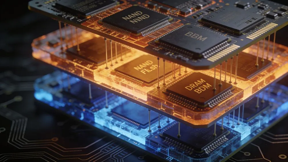
This is where SanDisk's HBF comes in. Instead of DRAM, it stacks NAND flash dies and connects them to the GPU via a UCIe interface. According to the specification (version 0.7.0) published through OCP (Open Compute Project) on August 3, 2026, HBF provides up to 512GiB of capacity and up to 3.072TB/s of bandwidth across 16 independent channel interfaces. NAND read latency is roughly 1,000 times that of DRAM (about 100 microseconds versus about 100 nanoseconds), but the design secures aggregate bandwidth by scheduling thousands of parallel reads simultaneously.
SanDisk and SK hynix are jointly driving this standardization effort, with Google and Tenstorrent also participating in the consortium. Commercialization is targeted for 2028 to 2029.
Point of Criticism 1: Comparing Against HBM Bandwidth Fixed 'Two Generations Behind'
The aspect of the Investor Day slides that drew the most criticism was the comparison that fixed HBM bandwidth at 12.8TB/s. This works out to 1.6TB/s per stack in an 8-stack configuration.
Let's check which generation this figure corresponds to. The HBM4 standard (JESD270-4) published by JEDEC in April 2025 specifies a 2048-bit interface with up to 8Gb/s per pin, yielding 2TB/s per stack. For 8 stacks, that's 16TB/s.
Meanwhile, the HBM4E controller IP announced by Rambus supports 16Gb/s per pin, achieving 4.1TB/s per stack and over 32TB/s in an 8-stack configuration. Samsung has also shipped 12-layer HBM4E samples in 2026, specifying pin speeds of 14-16Gb/s.
| Item | Value used by SanDisk | Projected value for 2028/2029 (HBM4E) | Difference |
|---|---|---|---|
| HBM bandwidth (per GPU) | 12.8 TB/s | 32 TB/s | ~2.5x |
| Bandwidth per stack | 1.6 TB/s | 4.1 TB/s | ~2.6x |
| Corresponding generation | HBM3E-equivalent | HBM4E | 2 generations |
Given that HBF's commercialization is slated for 2028/2029, the comparison target should be whichever HBM generation is mainstream at that time. Comparing HBF's maximum 3.072TB/s against HBM4E's 32TB/s widens the bandwidth gap to roughly 10x. Against the 12.8TB/s figure shown in SanDisk's slides, that gap appears to be only about 4x. The choice of comparison baseline alone dramatically changes HBF's relative appeal.
Point of Criticism 2: BF16, an Assumption 'No Longer in Use'
The second criticism concerns the choice of quantization precision. SanDisk's slides assumed that model weights would be stored in BF16 (16-bit floating point).
As of 2026, BF16 is already becoming a thing of the past in inference deployments. A large-scale empirical study presented at ACL 2025, encompassing over 500,000 evaluations, showed that FP8 (8-bit floating point) quantization of weights and activations is lossless across all model scales. NVIDIA's Blackwell architecture natively supports FP4, and NVIDIA's own benchmark materials for the Blackwell architecture state that running DeepSeek-R1 on B200 with NVFP4 achieves roughly 3x the token processing speed compared to FP8 on H200 (the published materials only state the ratio; the absolute tokens/s values for both the baseline and comparison cannot be confirmed from the sources referenced in this article).
The vLLM project's official blog from April 2026 also states explicitly that FP8 KV cache quantization is becoming the default in production environments.
Let's calculate concretely what this difference means. For the Qwen3-480B model:
| Quantization precision | Bytes per parameter | Total capacity for 480B parameters |
|---|---|---|
| BF16 | 2 bytes | 960 GB |
| FP8 | 1 byte | 480 GB |
| FP4 | 0.5 bytes | 240 GB |
Assuming BF16, a 480B model requires 960GB, which won't fit within 192GB of HBM by any stretch. Even HBF's 512GB isn't enough. But with FP8, only 480GB is needed, and with FP4, just 240GB—both of which fall well within the range that HBM alone, or HBM combined with HBF, can adequately cover.
The BF16 assumption works to maximize the apparent necessity of HBF. This is precisely why it's being criticized as choosing the 'most convenient assumption' for an investor presentation.
Point of Criticism 3: Write Endurance, the 'Elephant in the Room'
The third and perhaps most fundamental criticism is the complete omission of write endurance.
NAND flash cells have an upper limit on program/erase (P/E) cycles. TLC NAND typically caps out at 3,000 to 10,000 cycles, and even SLC maxes out at around 100,000. DRAM—that is, HBM—by contrast, has essentially unlimited write endurance.
Why could this difference be fatal? The KV cache is write-intensive data, with new entries added every time a token is generated during the decode phase of inference. Moreover, since the content differs with each request, reuse is difficult.
A paper published on arXiv on August 12, 2026, titled 'HBF Sucks! A Full-Stack Characterization of High-Bandwidth Flash for KV-Centric LLM Serving' (Zhuoran Li et al., Peking University), quantitatively examined this issue. The research team used an extended TokenSim simulator along with four types of two-hour production traces from Qwen-Bailian, five Dense/MoE models, and H100/B200 profiles to evaluate the use of HBF as an SSD-replacement KV cache layer.
The results are harsh. On both H100 and B200, average end-to-end latency increased by 2 to 5.5x, and the maximum throughput meeting SLO (Service Level Objective) requirements dropped by 1.1 to 2.7x. Across all traces, writes exceeded reads, and the 3D-ICE thermal model showed that the stack reaches its thermal limit before reaching peak bandwidth. In TLC configurations, HBF wears out faster than the SSD pool it's meant to replace.
The paper's conclusion is unambiguous: 'HBF is unsuitable as an SSD replacement for transient KV cache' (Finding 6: Without SSD-style write management, HBF is limited by write bandwidth and endurance, making it unsuitable for transient KV). However, it also notes that HBF is effective for read-only data like model weights, and that 'as a selective, reuse-aware, write-budgeted, and thermally-tuned tier, it has a place in LLM serving.'
Another paper presented at HotInfra 2026, 'Is High-Bandwidth Flash All You Need?', reaches a similar conclusion: 'HBF buys capacity, but NAND is write-limited at on-package decode-time scales. It cannot absorb the overflowing KV that grows as batches and contexts expand during decode, nor can it accommodate the expert pool reconfiguration that serving swaps demand.'
SanDisk itself has hinted at a direction that limits HBF's use to model weights. In an explanation positioned as something like the company's own technical blog, a division of labor was described: 'HBF is for AI model weights, HBM is for KV cache.' Nevertheless, this distinction was not made explicit in the Investor Day slides, which were structured in a way that gave the impression HBF also solves the KV cache problem.
What HBF Can Genuinely Solve
In fairness, let's also confirm HBF's legitimate use cases.
Model weights are essentially read-only once loaded at inference time. No write endurance issue arises. Moreover, with the spread of MoE (Mixture of Experts) architectures, it has become common for only a portion of the total parameters to actually be active (in the case of Qwen3-235B-A22B, only 22B of the 235B parameters are active). A design that offloads inactive expert weights to HBF and prefetches them as needed aligns well with HBF's strengths in both bandwidth and capacity.
As HyperAccel's technical blog laid out, there are three conditions under which HBF works: (1) the data must be read-only, (2) it must be loaded once and read multiple times, and (3) the access pattern must be predictable enough for prefetching to be effective. Model weights satisfy all three conditions. KV cache violates all three.
The OCP specification itself defines HBF as a 'non-coherent memory-centric flash device,' explicitly stating that its design is optimized for reads. While it specifies 4KiB-aligned burst lengths for writes, the specification does not include numerical endurance targets.
Between Investors and Engineers
Financially, SanDisk's Investor Day was a great success. An 80% gross margin target, roughly $94 billion in long-term contracts, and a 50% free cash flow margin. The stock has recovered more than 55% from its July lows.
However, the backlash from the tech community illuminates a different problem: the risk that investment decisions in AI inference infrastructure are being made without sufficiently scrutinizing technical details. Whether SanDisk's slides were 'wrong' will require awaiting the company's official response. As of August 14, 2026, SanDisk has not issued an official position on these criticisms.
One thing is certain: HBF is not a panacea that overcomes NAND's physical constraints—namely, write latency and endurance limits. It's a complementary technology that provides capacity HBM can't economically afford, for read-intensive workloads. If the narrative of 'breaking the memory wall' is pushed to the forefront without accurately conveying this positioning, the gap between expectations and reality will surface once commercialization arrives in 2028.
The arXiv paper's title is 'HBF Sucks!', but its subtitle is more precise: 'A Full-Stack Characterization'—a characterization across the entire stack. The value of a technology is properly assessed only when it's clear not just what it can solve, but also what it cannot. That latter half is precisely what was missing from the Investor Day slides.