

Samsung and Qualcomm Develop Organic Bridge Chip Tech to Bypass Intel's Packaging Patents
Translated from the Japanese original
Read the Japanese original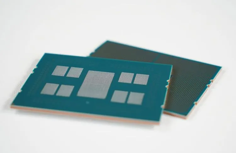
Samsung Electro-Mechanics has teamed up with Qualcomm of the United States to co-develop an advanced packaging technology for artificial intelligence (AI) semiconductors called the "2.1D Organic Bridge." The two companies have spent more than a year on development and validation, and Samsung Electro-Mechanics publicly unveiled the related substrate technology for the first time at KPCA Show 2026, held September 9-11, 2026. By eliminating the costly silicon interposer and connecting dies directly, this approach raises the question of how it might reshape both the cost structure and the patent landscape of advanced packaging.
## A 2.1D Structure That Eliminates the Interposer, and the Background to the Partnership
With the expansion of generative AI, advanced packaging that links multiple compute dies—or connects a GPU to high-bandwidth memory (HBM)—with wide bandwidth and low latency has become essential for AI accelerators and data center processors. The dominant approach until now, 2.5D packaging (such as TSMC's CoWoS-S), places a silicon interposer atop the substrate and arranges chips on top of it. However, interposers, which are fabricated from large silicon wafers, are extremely expensive, and area limitations imposed by lithography mask sizes (reticle limits) as well as declining yields have consistently constrained manufacturing.
A technique known as "2.1D packaging" has emerged as a solution to this challenge. In 2.1D packaging, a full-surface silicon interposer is not used. Instead, ultra-compact relay components called "bridges" are placed only at the die boundaries that require high-density wiring, directly linking the chips.
Samsung Electro-Mechanics has developed a technology that forms these bridges not from conventional silicon but from "organic materials" derived from printed circuit board (PCB) material technology. A cavity is carved into the flip-chip ball grid array (FC-BGA) substrate that holds the chip, and a miniature organic bridge is pre-embedded into that cavity. Qualcomm's compute die and other components are then mounted on top, achieving high-density multi-die integration without an interposer.
The two companies have spent over a year evaluating the electrical performance, thermal cycling, and bonding reliability of substrates using this configuration. The unusual pairing—with fabless semiconductor company Qualcomm taking the lead on packaging-related core technology and major substrate maker Samsung Electro-Mechanics handling implementation—stems from a strong shared motivation to control back-end packaging costs and supply chains independently.
## From Silicon to Organic: The Structure and Fine-Pitch Specifications of the Organic Bridge
The organic bridge is essentially an ultra-small substrate equipped with extremely fine multilayer wiring. Qualcomm's published interconnect bridge patent (US20260101781A1) discloses a structure in which a "metal-dielectric composite structure" (redistribution layer, or RDL)—formed by alternately patterning metal and dielectric layers—is bonded to an "organic structural layer" such as mold resin, with through-layer interconnects passing through the organic layer to electrically connect to wiring on the package substrate side.
The design specification Samsung Electro-Mechanics is targeting calls for an RDL circuit structure with 5 to 7 layers. The company aims for extreme miniaturization, with a circuit line width and spacing (line/space, or L/S) of 1.5 to 2.0 μm, and via diameters connecting the layers of 4 to 5 μm. This would allow the wiring pattern density at the die-to-die boundary to reach 500 to 1,000 lines per millimeter of width.
The build-up wiring layers typically used in standard FC-BGA substrates are limited to line widths of around 10 μm at their finest. As a result, attempting to connect dies directly using only substrate-side wiring would fail to provide enough signal lines, causing a critical bandwidth shortfall. By contrast, the organic bridge's L/S density of 1.5 to 2.0 μm rivals the wiring technology formed on silicon wafers. By concentrating fine wiring on the organic bridge side, it becomes possible to create localized high-density signal transmission paths without having to push the design rules of the FC-BGA substrate itself to their absolute limits.
On the manufacturing and supply chain front as well, Samsung Electro-Mechanics is proceeding with careful validation. The company is evaluating two parallel supply routes for the organic bridge: in-house manufacturing and external procurement. While a small number of evaluation bridges are being prototyped on the company's own pilot line, evaluation samples are also being produced at DSRJ (Device Solutions R&D Japan), a Japan-based research site under the Samsung Advanced Institute of Technology (SAIT). Additionally, a process is being validated in which organic bridges manufactured by external substrate and materials partner companies are procured and embedded into Samsung Electro-Mechanics' FC-BGA substrates. This appears aimed at avoiding concentration in a single facility and securing early yield stability and supply reliability ahead of mass production.
## Why Organic? Bypassing Intel's EMIB Patents and Shifting the Cost Structure
Why is the semiconductor industry pursuing an organic bridge rather than the proven silicon alternative? The main reasons are lower manufacturing costs and avoidance of an existing patent network.
The basic concept of embedding a small bridge in a substrate to connect chips was pioneered by Intel's "EMIB" (Embedded Multi-die Interconnect Bridge), commercialized starting in 2017. However, EMIB relies on a silicon micro-chip (a silicon bridge). While silicon bridges offer excellent fine-pitch capability, they must be manufactured using front-end semiconductor fab processes—exposing and etching fine circuits onto a wafer. This entails expensive wafer processing costs, and embedding silicon pieces into a substrate requires sophisticated manufacturing control to manage stress concentration and warping caused by differences in coefficient of thermal expansion (CTE).
In addition, Intel has spent years building a robust and extensive patent network covering EMIB's basic structure and embedding methods. Any competitor or fabless company seeking to adopt a silicon bridge approach faces a constant risk of infringing on Intel's intellectual property (IP).
The organic bridge offers a counter-approach that overcomes both barriers. Because it doesn't require front-end semiconductor fabrication equipment and can instead be produced using RDL technology extended from PCB and package substrate manufacturing processes, it can significantly reduce manufacturing costs. Most importantly, by constructing the bridge's core material from organic polymer materials and copper wiring, it becomes possible to legally circumvent Intel's silicon-bridge-related patent network.
The 2.1D structure—placing inexpensive organic bridges only where high-density connections are needed while completely eliminating the silicon interposer—represents a practical solution that big tech companies have long sought amid the enormous costs of advanced packaging.
## Gaps Between the Original Announcement, Patent Filings, and Initial Reporting, and the Division of Roles
An interesting gap in disclosure exists among the official corporate announcement, publicly available patent information, and investigative reporting surrounding this 2.1D organic bridge development.
First, Samsung Electro-Mechanics' official announcement at KPCA Show 2026 revealed the exhibition of 2.1D package substrate technology that directly connects chips without a silicon interposer, but it kept entirely confidential any specific customer names or the existence of a co-development partner. Meanwhile, Qualcomm had filed an interconnect bridge patent (US20260101781A1, published April 2026) in October 2024 combining an organic structural layer with a composite wiring layer, steadily solidifying its own proprietary bridge architecture. It was a scoop from South Korea's The Elec that connected these dots, reporting that Samsung Electro-Mechanics and Qualcomm had been jointly evaluating organic bridge-embedded FC-BGA substrates for over a year.
Particularly important within this collaborative framework is the clear division of roles within the Samsung group. Samsung Electro-Mechanics handles the physical manufacturing of the FC-BGA substrate and the embedding of the organic bridge into the cavity, while Samsung Electronics' Foundry division is responsible for the comprehensive evaluation of overall package assembly performance and thermal/mechanical reliability in the back-end process.
Some overseas breaking news reports mistakenly identified Samsung Electronics Foundry as the manufacturing entity, but in reality, this substrate technology is led by Samsung Electro-Mechanics, a company specializing in electronic components and substrates. Samsung Electronics Foundry positions itself as an evaluation partner seeking to expand its foundry service offerings by linking its own advanced packaging portfolio—including the silicon-bridge-based Cube-E and the organic RDL interposer-based Cube-R—with Samsung Electro-Mechanics' 2.1D substrate.
## Qualcomm's Data Center AI Strategy and the Road Ahead for Commercialization
Partner Qualcomm's objective is unmistakably clear. While the company maintains its leadership in smartphone SoCs, it has been ramping up development of large-scale, multi-die AI accelerators for data centers. Following its October 2024 patent filing, Qualcomm hired advanced packaging engineers in South Korea in March 2026 who are well-versed in organic bridge technology.
Qualcomm's goal is to densely tile multiple compute dies using organic bridges to realize a multi-die AI processor that behaves, from a software perspective, as a single massive accelerator. As a fabless company without its own fab, this suggests an intent to break away from dependence on TSMC alone for packaging and to establish an independent supply route by partnering with Samsung Electro-Mechanics and Samsung Electronics Foundry.
That said, technical hurdles remain on the path to commercialization. Organic materials have a higher coefficient of thermal expansion than silicon, and under the high-heat operating conditions of AI accelerators, fine-pitch bonding joints are prone to fatigue failure and substrate warping from prolonged thermal cycling. Whether the target L/S of 1.5 to 2.0 μm can be maintained defect-free at mass-production scale with high yield also remains an open question.
When will a technology validated over more than a year make its way into commercial products? The 2.1D organic bridge, which addresses cost and patent constraints simultaneously, offers a new option in the power balance of AI semiconductor packaging currently dominated by TSMC.