


You may have heard the term "terahertz waves" at an airport security checkpoint. Some security scanners that see through clothing to detect explosives or drugs already use this type of electromagnetic wave. Yet the equipment involved is roughly the size of a washing machine, with price tags starting in the tens of millions of yen. Why has such a compelling technology remained so "cumbersome" for so long? The answer lies not in the electromagnetic wave itself, but in a long-standing barrier in how the devices that handle it are built.
Why the "Blind Spot" of the Electromagnetic Spectrum Went Unfilled for 30 Years
Within the electromagnetic spectrum, the terahertz band (0.1 to 10 terahertz) remained largely untouched for a long time. Higher in frequency than microwaves but lower than infrared light, this band was once known as the "terahertz gap." For electronic devices, the frequencies were too high to handle easily; for optical devices, the wavelengths were too long to control effectively. To engineers on either side, terahertz was always someone else's problem.
When early terahertz systems began operating in laboratories in the 1990s, the potential of this band became immediately apparent. Like radio waves, terahertz waves can pass through walls, yet unlike X-rays, they don't emit dangerous ionizing radiation. They can non-invasively measure the water content of biological tissue, visualize defects in semiconductors, and examine the internal structure of cultural artifacts without damaging them. Because the frequencies are higher, they can also secure far broader bandwidth than microwaves or millimeter waves, making wireless communication speeds approaching terabits per second theoretically achievable. In the ongoing research into 6G communications, the sub-terahertz to low-terahertz band (roughly 0.1 to 1 THz) is emerging as a leading candidate—which is precisely why research institutions around the world are racing to develop this technology.
And yet, even after 30 years, terahertz systems have failed to leave the laboratory. The barrier lay not so much in physical theory as in engineering implementation. Systems of that era were built by lining up multiple discrete components—lasers, amplifiers, modulators, terahertz signal sources, and detectors—using precision optical components arranged in series. Each component came from a different manufacturer, required manual alignment at the micron scale, and demanded readjustment every time the temperature changed. This was not a structure that could survive outside the lab.
Prior work in the photonics field had repeatedly attempted "modular integration," but many of the materials suited to terahertz generation and detection were incompatible with standard semiconductor fabrication lines. For example, low-temperature-grown GaAs (LT-GaAs), which offers high conversion efficiency, requires dedicated equipment and processes for epitaxial growth; attempting to incorporate it into silicon photonics or general InP processes causes manufacturing costs to skyrocket. A material barrier stood doubly in the way, layered on top of the system integration barrier.
The Reverse Insight: "Repurposing" Quantum Wells
The path chosen by the team at UCLA's Terahertz Electronics Lab, led by Professor Mona Jarrahi, was to reframe the problem itself. Rather than starting from specialized materials dedicated to terahertz applications, they pursued the question of whether quantum well PIN photodiodes—already mass-produced as standard components in the photonic integrated circuit (PIC) industry—could also handle terahertz signal processing.
A quantum well is a structure made of ultra-thin semiconductor layers (each only tens of atoms thick) stacked together, which exploits the quantum mechanical behavior of electrons to precisely control light. It has served for decades as the heart of high-speed lasers and modulators used in optical communications, with an extensive manufacturing track record. The attempt to repurpose this material—from its "original purpose in optical communications" to "terahertz generation and detection"—forms the core of this research.
What the team implemented is a technique called "gain-enhanced interband photomixing." When two laser beams are overlapped within a quantum well structure, a signal corresponding to their frequency difference is generated. For instance, if the two lasers are tuned so their frequency difference equals 1 terahertz, a 1-terahertz signal can be extracted. The key lies in the "gain-enhanced" part: because the quantum well structure amplifies light while performing photomixing, it can generate signals more efficiently than conventional optical-interference-based photomixers. Since the same structure also functions as a detector, a single device can handle both transmission and reception.
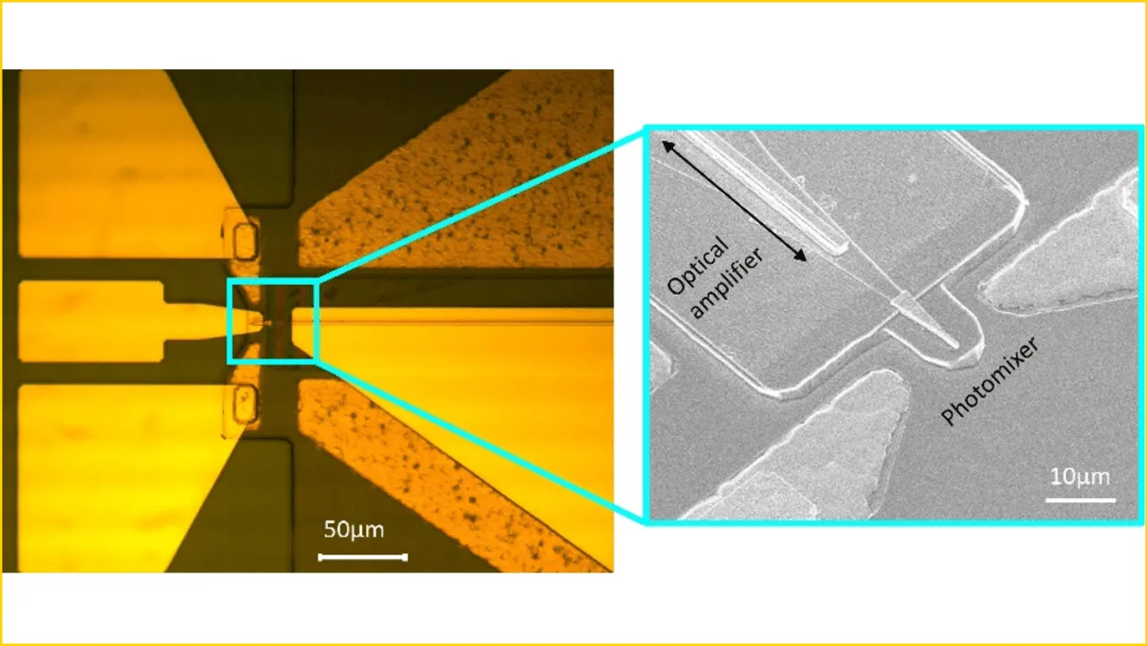
The research team named this approach the "MITO (Monolithically Integrated Terahertz Optoelectronic)" platform. Four functions—signal generation, detection, modulation, and amplification—are integrated monolithically, meaning seamlessly, onto a single chip. The starting point for this research is the striking fact that functionality which once occupied an entire optical table in a laboratory now fits on a fingertip.
What Changes When It All Fits on One Chip
Considering the concrete implications of manufacturing compatibility reveals the true scope of this research.
First, there's a change in scale. Conventional terahertz systems resemble the era just before refrigerator-sized computers became desktop microprocessors. Just as 1970s mainframes occupied entire rooms, today's terahertz equipment requires large optical tables and can weigh tens of kilograms. Just as electronic integrated circuits democratized computing by consolidating transistors onto a single chip, terahertz integration holds the potential to dramatically reduce system weight, power consumption, and cost. If mass production becomes feasible, a path opens for unit costs to shift gradually from today's specialized-equipment price range down toward the cost level of consumer chips.
Next is the matter of cost and mass production. The quantum well PIN PIC process used by this team is a well-established method within the optical communications industry. This suggests that manufacturing can proceed simply by handing design data to an existing foundry, without the need to build a new dedicated production line. Past attempts at single-chip integration were hampered because the use of terahertz-specific materials prevented alignment with standard processes, leaving no clear path to mass production. The greatest significance of this work lies in having overcome that barrier while standing on the foundation of industry standards.
The scope of potential applications also broadens. If highly sensitive, compact terahertz sensors become available at low cost, applications such as wearable imagers for early cancer screening, non-destructive inspection equipment on factory lines, or chemical-monitoring features embedded in smartphones start to feel within reach. As for integration into 6G base stations—a role that demands highly efficient coupling with optical fiber—this platform is also emerging as a strong candidate. Being able to use a common chip platform across multiple applications would also offer a significant advantage in terms of spreading out development costs.
| Item | Conventional Terahertz Systems | This Study's MITO Platform |
|---|---|---|
| System scale | Occupies a large optical table (weight: tens of kg) | A single semiconductor chip (fingertip-sized) |
| Component configuration | Five or more discrete components, manually aligned with precision | Four functions integrated monolithically (seamless) |
| Manufacturing process | Terahertz-specific materials, custom processes | Compatible with industry-standard PIC processes |
| Estimated cost range | Device unit price: tens of millions to hundreds of millions of yen | Path exists toward consumer-chip cost levels at mass-production scale |
Barriers Not Yet Crossed
What this research demonstrates is a "proof of principle," not a finished product.
What has been publicly disclosed so far is the fact that this approach achieves more efficient terahertz generation and more sensitive detection compared to existing photomixer-based technologies. However, the paper does not reveal specifications such as the chip's operating bandwidth, concrete conversion efficiency figures, or coupling losses to and from other chips. This is a demonstration from a single laboratory, and reproducibility across different manufacturing lots or operating environments has not yet been confirmed. While the work has been published as a peer-reviewed paper, reports of independent replication or third-party verification will have to wait for the future.
Power consumption also remains an unresolved variable. The photomixing architecture, which requires two lasers, poses power-efficiency challenges for future integration into ultra-compact devices. Whether it will be possible to generate a target frequency directly from a single laser source, or to integrate an on-chip light source, remains a research question for the medium to long term. Additionally, exactly how much of the 0.1 to 10 THz range this quantum well structure can effectively cover will require more detailed specification disclosures.
For terahertz technology to truly complete the shift "from the optical table to the fingertip," three stages must be traversed: proof of principle at the chip level, mass production with stable yields, and finally, performance assurance in real-world environments. This research has certainly marked the starting point of that journey. The next question will be answered by the production line.