

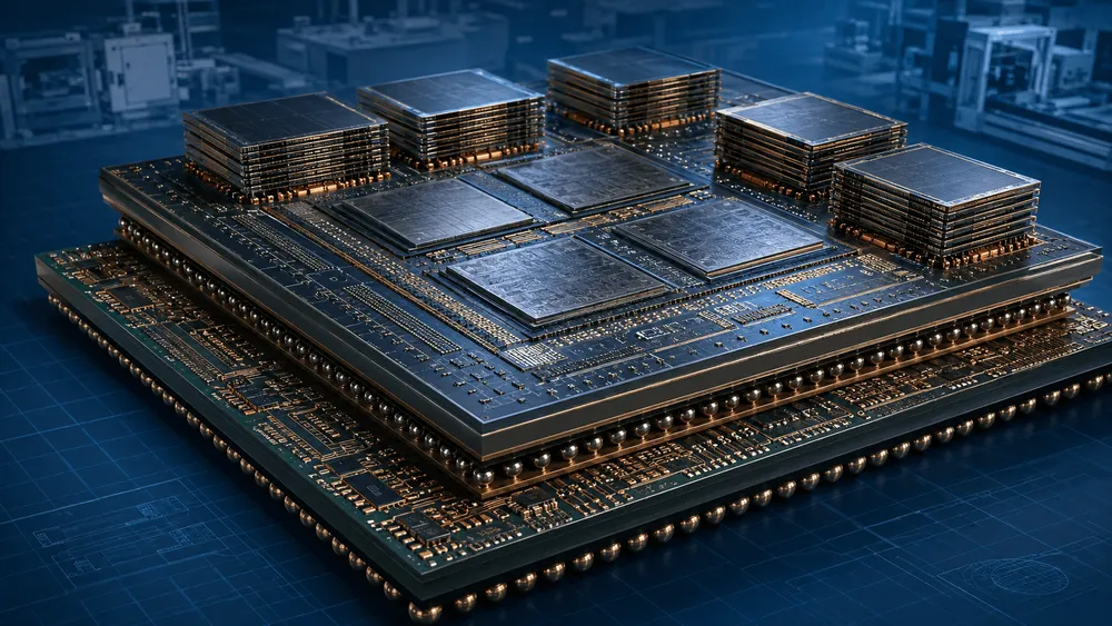
TSMC has cleared one of the major hurdles in CoWoS, the packaging technology used to assemble large AI chips. At the OCP APAC Summit on August 11, 2026, Jun He, the company's Vice President of Advanced Packaging Technology and Services, explained that 5.5x reticle-size products have stably achieved yields exceeding 98% across multiple AI customer products, with some reaching as high as 99%. However, high yield does not mean AI accelerators can be shipped in the volumes needed. TSMC's mention of memory and ABF substrate shortages, material variability, and system-level reliability in the same presentation made clear that the supply bottleneck is moving from inside the CoWoS process to the surrounding components and validation work.
The 99% figure comes with a caveat. According to on-site reporting by Economic Daily News, the common benchmark across multiple products is "stably above 98%," with 99% being the peak achieved by only some products. TSMC has not disclosed the denominator used for yield calculations, nor which stage of the process the figures cover. While this cannot be read as the pass rate for complete AI systems, it does offer new insight into mass-production maturity that wasn't revealed in the company's official announcement in May 2026.
5.5x Reticle Size Is Approximately 4,565 Square Millimeters
A reticle refers to the maximum area a lithography tool can transfer in a single exposure. TSMC defines one reticle as approximately 830 square millimeters, so at 5.5x, the interposer-equivalent area comes to roughly 4,565 square millimeters by simple calculation. This does not represent the overall package dimensions including the housing. Still, it indicates the scale involved in placing compute dies and high-bandwidth memory (HBM) side by side—far exceeding the area of a single leading-edge logic die—and connecting them with short interconnects.
CoWoS-L has been the technology enabling this expansion. While conventional CoWoS-S uses a large silicon interposer, CoWoS-L embeds local silicon interconnects (LSI) within a redistribution layer (RDL), placing silicon only where fine-pitch wiring is needed. According to TSMC's annual report, 3.5x reticle CoWoS-L entered mass production in 2024. The progress highlighted here is the expansion to 5.5x within two years, while maintaining yields above 98% across multiple products.
| Year | TSMC's Plans/Achievements | Packaging-Side Changes |
|---|---|---|
| 2024 | 3.5x CoWoS-L enters mass production | Scaling up via RDL and LSI |
| 2026 | 5.5x product in mass production; yields above 98% across multiple products | Area equivalent to approximately 4,565 square millimeters |
| 2028 | 14x product planned for mass production | Integrating roughly 10 large compute dies and 20 HBM units |
| 2029 | Expansion beyond 14x; 40x-equivalent SoW-X also planned | Transition from packaging to wafer-scale systems |
The key takeaway from this table isn't a record-breaking area figure. Rather, it's that over the four years from 2024 to 2028, the number of compute dies and memory units mounted on CoWoS will increase, rapidly intensifying the interdependencies spanning materials, power, heat dissipation, and inspection. The high yield of the 5.5x product represents a necessary condition for advancing to the next stage of scaling.
As Yield Rises, Supply Constraints Shift Outward
CoWoS process yield determines what proportion of input components can be finished as viable packages. Shipment volumes, however, are also determined by whether good compute dies, the required quantity of HBM, and large ABF substrates all become available at the same time. Even if the CoWoS process stabilizes above 98%, assembly cannot begin without HBM on hand. The same holds true if large ABF substrates are in short supply.
On the memory side, tightness isn't limited to HBM. In its June 2026 earnings call, Micron projected that supply-demand conditions for DRAM and NAND would remain tight even beyond 2027. The company has multi-year supply agreements allocating DRAM and NAND—including HBM—to customers. The fact that customers have already secured memory generations several steps ahead illustrates why increased CoWoS capacity doesn't automatically translate into higher AI chip output.
For ABF substrates, both area and layer count are driving up demand. ABF (Ajinomoto Build-up Film) is used in the fine-wiring layers of organic substrates that connect the interposer—carrying compute dies and HBM—to the server board. In its June 2026 business briefing, Ajinomoto explained that as high-performance semiconductors grow larger and more layered, ABF consumption per package is increasing. The company plans to incrementally expand supply capacity at facilities including its Gunma plant through 2030, and is also planning a third site with capacity equivalent to the Gunma plant to meet demand beyond 2030.
Ibiden's plans, as a substrate manufacturer, further illustrate the timing gap. The company forecasts that demand for SAP (semi-additive process) processing for large, multi-layer substrates will exceed industry-wide supply capacity, and plans to raise its capacity index—set at 1 for 2024—to 1.8 by 2026 and 2.5 by 2028. While the company is investing a total of 500 billion yen in its Kawama and Ohno plants in Gifu Prefecture, mass production from the new equipment will only begin incrementally starting in fiscal 2027. Demand is rising now, meaning it will take at least a fiscal year or more before the effects of this capacity expansion become substantial.
Multi-Sourcing Narrows the CoWoS Process Window
The natural response to supply shortages is to source the same component from multiple suppliers. However, with large-scale CoWoS, adding more suppliers actually complicates manufacturing conditions. According to Jun He, ABF substrates vary in thermal and mechanical properties depending on the manufacturer, and these differences narrow the CoWoS process window—the range of thermal and mechanical conditions within which good yield can be reliably achieved. Coplanarity, or maintaining a uniform height across connection surfaces, also tends to deteriorate during final assembly.
The root cause lies in the size of the package. Silicon and RDL expand and contract differently under heating and cooling compared to organic substrates and printed circuit boards. As the area increases, so does the stress and warpage caused by differences in thermal expansion coefficients, which in turn affects lid placement, thermal interface material (TIM), and even the layout of passive components. Substrates that appear interchangeable from a procurement standpoint may not simply drop into existing temperature profiles or fixtures.
An example presented at the event illustrates why this problem is hard to catch through component-level testing alone. When the same chip was integrated into different systems, damage appeared at die edges that hadn't shown up during component testing—prompting TSMC and the customer to adjust the printed circuit board, passive component layout, and manufacturing process. Conversely, stress detected at the component stage sometimes disappeared after mounting onto the substrate. Without accounting for actual mechanical constraints, cooling conditions, and the influence of the printed circuit board and system structure, failure conditions simply cannot be reproduced.
This is why TSMC is bringing System Technology Co-Optimization (STCO) into play before mass production begins. The company also noted that keeping failure rates for large AI systems within acceptable limits requires individual packaging components to meet quality standards exceeding even those for automotive applications. The next metrics to track, beyond the 98%+ process yield, are process capability when switching materials and long-term reliability in actual systems.
System Boundary Conditions Ahead of Component Testing
TSMC's policy is to publish system boundary conditions six quarters—roughly 18 months—before mass production, gathering feedback from customers and the industry. In a development approach where technology, manufacturing, and customer teams work sequentially, the timeline wouldn't keep pace with annually updated AI products. Instead, material suppliers, equipment makers, and system integrators need to advance prototyping and validation simultaneously, feeding real-world conditions—including warpage and cooling, in addition to temperature and load—back into the manufacturing process.
This development approach is also tied to the supply problem. Adopting an alternative ABF substrate requires more than just matching material specifications—the package using that substrate must be validated with actual boards and cooling structures. While adding more suppliers reduces volume risk, it also increases the number of combinations that need qualification. The effectiveness of multi-sourcing isn't determined by the number of suppliers, but by the volume of qualified components that can share the same mass-production conditions.
The planned 14x CoWoS for 2028 will integrate roughly 10 large compute dies and 20 HBM units into a single package. What needs to be verified here isn't whether peak yield reaches 99%. Rather, it's how far the range of "above 98% across multiple products" can be extended, whether substrate capacity expansion starting in fiscal 2027 will come online with proper qualification, and whether multi-year memory contracts will meet the required volumes for next-generation HBM. Only when all three of these conditions align will the massively scaled-up CoWoS transform from a roadmap area figure into deployable AI computing capacity.