

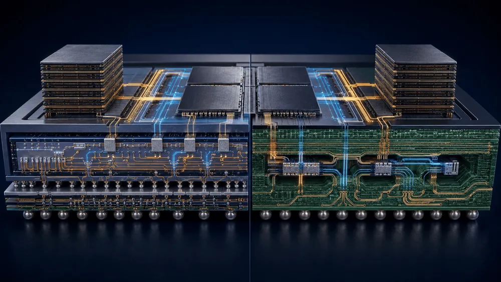
TSMC is reportedly developing an advanced packaging technology similar to Intel's Embedded Multi-die Interconnect Bridge (EMIB). The Information reported this on July 30, 2026, citing two people with direct knowledge of the project. It's also reported that TSMC is collaborating with substrate maker Kinsus Interconnect Technology, though neither TSMC nor Kinsus has publicly disclosed the project. The name, structure, and mass production timeline have not yet been disclosed.
This move can't be fully understood as simply TSMC replicating Intel's bridge-type packaging. TSMC's CoWoS-L also places small silicon bridges exactly where needed to connect dies. What distinguishes the two approaches is which layer of the package the bridge is embedded into, and who runs mass production for the processes before and after that step.
Two Sources Describe a Technology 'Similar to Intel's'
According to The Information's account, TSMC is developing an advanced packaging technology similar to an approach Intel already offers, and the publication frames this as a sign that TSMC is wary of competition from Intel. It also reported that TSMC is working with Kinsus. However, no official name has been confirmed, so it cannot yet be treated as a specific named product.
The reported collaboration with Kinsus offers a clue to the technical direction. The company supplies FCBGA substrates not only for microprocessors and GPUs but also for ASICs and FPGAs, and it cites fine pitch and high layer counts as its distinguishing features. That said, it remains unclear whether Kinsus will simply supply substrates or will also handle process development and ramp-up to mass production.
The report also doesn't confirm that an RDL interposer would be eliminated entirely. Collaboration with a substrate maker is consistent with changes on the substrate side, but that alone doesn't establish the layer configuration, which TSMC has not disclosed.
CoWoS-L Already Uses Localized Silicon Bridges
Reading TSMC's official explanations, CoWoS-L is not a "full-interposer approach" unrelated to EMIB. Whereas CoWoS-S uses a large-area silicon interposer, CoWoS-L embeds a Local Silicon Interconnect (LSI) into a molded RDL interposer. Submicron copper wiring within the LSI connects SoCs to each other, or SoCs to HBM, at high density exactly where needed.
The first 3.5x reticle-size CoWoS-L entered mass production in 2024. CoWoS-S has been in mass production since 2012 and currently accommodates a silicon interposer up to 3.3x reticle size, or roughly 2,700 square millimeters. For larger AI accelerators, TSMC recommends either CoWoS-L or CoWoS-R, which uses RDL-based wiring.
| Approach | Localized High-Density Connection | Layer Where Bridge/Wiring Is Placed | Publicly Confirmed Stage |
|---|---|---|---|
| TSMC CoWoS-S | Large-area silicon interposer | Between die and substrate | Mass production since 2012 |
| TSMC CoWoS-L | LSI silicon bridge | RDL-based intermediate interposer | 3.5x reticle products in mass production since 2024 |
| Intel EMIB | Small silicon bridge | Within the package substrate | Mass production since 2017 |
| Reported new TSMC approach | Said to resemble Intel's approach | Undisclosed | Reported to be under development |
In other words, what remains undisclosed isn't the fact that "TSMC also uses silicon bridges." It's whether the bridge will be placed closer to the substrate than in existing CoWoS-L, and how the intermediate interposer and assembly process would be changed.
EMIB Embeds the Bridge Within the Package Substrate
Intel's EMIB places a small silicon bridge into a cavity formed in the substrate, integrating it with dielectric and metal build-up layers. Fine microbumps are only required around the bridge itself, allowing the rest of the die to maintain a coarser bump pitch. Rather than routing through a large-area silicon interposer, this design connects adjacent logic dies to each other, or logic to HBM, exactly where needed.
Intel has mass-produced EMIB since 2017 and has expanded it into EMIB-M, which adds MIM capacitors to supplement power delivery, and EMIB-T, which runs TSVs through the silicon bridge. In a research demonstration presented at ECTC 2026, EMIB-T showed a 25µm FLI bump pitch, a 120×120mm package, and compute/memory silicon exceeding 9x reticle size. Bandwidth figures cited include over 12Gb/s for HBM4e and 64Gb/s for UCIe.
These are Intel's own research figures, not measured numbers showing superiority over TSMC in any specific customer's mass-produced product. Still, they indicate that EMIB is advancing toward technology development targeting large AI packages. In an actual transition, work would also be needed to align package design rules and verify compatibility with HBM. Maximum area alone doesn't determine adoption.
TSMC Welcomes EMIB-T While Intel Expands Its Manufacturing Network
TSMC CEO C.C. Wei was asked about EMIB-T as a competitive threat during the Q2 2026 earnings call on July 16. Wei acknowledged that TSMC's packaging capacity is tight enough to constrain customer growth, and said he welcomes more options in the market. The logic is that if competitors take on back-end packaging load, it becomes easier to get TSMC-made wafers into products, which in turn grows TSMC's core front-end business.
Intel, meanwhile, is expanding its manufacturing network in parallel with bridge design work. In April 2025, Amkor announced it would expand EMIB assembly capacity in South Korea, Portugal, and the United States through a strategic partnership with Intel. If external assembly sites are available in addition to Intel's own internal facilities, customers can evaluate technology and supply capacity together.
The Information reported in June that Google and Nvidia were considering Intel as a backup manufacturing source, and that SK hynix was also testing whether its own memory would reliably work with Intel's advanced packaging. None of this confirms adoption or mass production has been finalized. However, it does show that the "alternative back-end route" that TSMC said it welcomed has begun to become something customers are actually evaluating and testing.
Not to Be Confused with a Separate, About-a-Year-Out Project
On the same July 16 earnings call, TSMC also answered questions about glass substrates and glass cores. According to Wei, CoWoS remains the current mainstay, and the company is developing a lower-cost alternative technology together with substrate vendors. He said the pilot line would take about a year to reach a maturity level usable for production with customers.
This statement made no mention of Kinsus or EMIB. TSMC has not confirmed that this is the same project as the EMIB-like effort reported two weeks later, so the roughly one-year timeline cannot be carried over to a mass-production schedule for the new approach.
The new approach can only be properly evaluated once TSMC discloses the cross-sectional structure and the mass-production process. Will an RDL interposer be retained? Which layer will Kinsus manufacture? How much of an existing CoWoS-oriented design can customers carry over unchanged? Once these details are made public, it will become possible to determine whether TSMC's development effort is an additional line to fill a capacity shortfall, or a new product line built to compete head-on with EMIB.