

テクノロジー
NVIDIAがcuFile APIをオープンソース化、GPUがストレージを直接駆動する時代へ
NVIDIAがGPU用ストレージ直接アクセスAPI「cuFile」をオープンソース化し、GPUがCPUを介さずストレージI/Oを制御するSCADAアーキテクチャの標準化を40社超で推進。AI推論のボトルネックが計算からデータ供給に移る中、ストレージ業界の構造変化が始まる。

KIOXIA(キオクシア)は、東芝のメモリ事業を継承して設立された日本の半導体メーカーである。NAND型フラッシュメモリの発明企業としての系譜を持ち、SSDをはじめとする幅広いストレージ製品を設計・製造している。本社は東京都に置かれ、東京証券取引所に上場している。
KIOXIAは半導体産業に属し、NAND型フラッシュメモリの開発・製造で世界的な地位を占める企業である。データセンター向けエンタープライズSSDから、PCやスマートフォン向けのクライアントSSDまで、用途に応じた多様なストレージソリューションを提供している。旧東芝メモリとして培った製造技術と量産体制を基盤に、Samsung、SK hynix、Western Digitalといった競合と並ぶNAND大手として位置づけられている。
同社の起源は東芝のメモリ事業にある。2017年1月に東芝メモリとして分社化され、2019年1月に社名をKIOXIAへ改称した。この改称を法人としての実質的な設立と位置づける資料もあり、Wikidata上でも2017年と2019年の双方が設立日として記録されている。以降、独立した半導体メーカーとしてNAND型フラッシュメモリおよびSSD事業を継続してきた。
NAND型フラッシュメモリはSSDやメモリカード、スマートフォンのストレージなど広範な用途に組み込まれる基盤技術であり、KIOXIAはその発明企業としての歴史的優位性を持つ。近年はAI関連インフラの拡大により、データセンターでの大容量ストレージ需要が急増し、NAND市場全体の供給構造に大きな影響を及ぼしている。KIOXIAはこうした需要変化に対応するため、PCIe対応の高速SSDやQLC NANDを採用したコストパフォーマンス重視の製品など、複数の技術方針を並行して展開している。
2026年6月には、KIOXIAがクライアント向けSSDの新シリーズ「KIOXIA BG8」と「KIOXIA EG7」を発表したことが報じられた。BG8はPCIe 5.0対応でメインストリームPC向けに高速ストレージを提供し、EG7はQLC NANDを採用してコストパフォーマンスを追求する製品である。両シリーズともDRAMレス設計とHMB技術を採用し、総所有コストの最適化を図っている点が特徴とされる。
同時期には、AI需要による部材不足を背景に、2026年のSSD市況に関する報道も相次いだ。2026年6月3日の記事では、かつて手頃な価格帯にあった1TB級SSDの価格帯が崩れつつあるとの指摘があり、KIOXIAから発せられたNAND需給に関する警告が業界に波紋を広げたことが伝えられた。さらに2026年6月8日には、SamsungやSK hynixとともにKIOXIAがNANDの協調減産に動いているとの報道があり、SSD価格のさらなる高騰要因として挙げられている。同じ時期にSK hynixがDRAM生産能力の増強とNAND事業の戦略的縮小を進めているとの報道もあり、メモリ業界全体でAI需要への対応が生産戦略の再編を促している状況がうかがえる。
こうした需給環境の変化は、PC市場にも影響を及ぼしている。IDCの予測を紹介した記事では、メモリ価格の高騰が2026年後半のPC平均販売価格を押し上げ、出荷台数の減少にもつながる見通しが示された。KIOXIAを含むNANDメーカー各社の生産・価格戦略は、こうしたエンドユーザー向け製品市場の動向とも密接に結びついている。
NVIDIAがGPU用ストレージ直接アクセスAPI「cuFile」をオープンソース化し、GPUがCPUを介さずストレージI/Oを制御するSCADAアーキテクチャの標準化を40社超で推進。AI推論のボトルネックが計算からデータ供給に移る中、ストレージ業界の構造変化が始まる。

超党派上院議員6名がAppleに中国CXMTとYMTC製メモリの不使用を8月21日までに確約するよう求めた書簡を、2022年のYMTC撤回劇や書簡署名議員の地元投資利害と重ねて読み解く。AI逼迫とMicronの2500億ドル投資も焦点。
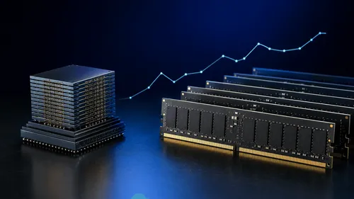
SK hynixの2026年4〜6月期決算は、売上高と営業利益で過去最高を更新したが、汎用DRAMの急騰や製品構成の変化により市場予想には届かなかった。HBMの価格体系や出荷時期のずれが影響したものの、高い利益率と財務余力を背景に次世代製品への投資を加速させる方針だ。

IDCの予測によれば、部材不足やAI需要に伴うメモリ価格の高騰により、2026年のPC平均販売価格は17%上昇し出荷台数も大幅に減少する見通しだ。低価格モデルの投入も期待されるが、2027年末までは構成の妥協や実質的な値上がりが続く。

PCI-SIGは、x16構成で最大1TB/sの双方向帯域幅を提供するPCIe 8.0の仕様ドラフト0.5を前倒しで公開し、2028年の最終仕様策定を目指している。この規格は、256 GT/sへの高速化に伴う信号減衰を克服するため、PAM4シグナリングやFLITエンコーディングを維持しつつ、下位互換性を保ちながら新たな物理コネクタ技術の評価を進めている。
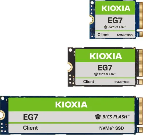
AIインフラ特需による部品価格高騰がコンシューマーPC市場に逆風となる中、キオクシアはクライアント向けSSDの新シリーズ「KIOXIA BG8」と「KIOXIA EG7」を発表した。BG8はPCIe 5.0対応でメインストリームPCに高速ストレージをもたらし、EG7はQLC NAND採用でコストパフォーマンスを追求しつつ、両シリーズともにDRAMレス設計とHMB技術でTCOを最適化している。
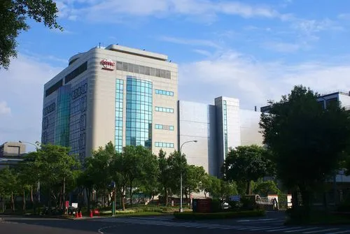
TSMCはA13プロセス技術を発表したが、これはA14の後継ではなく、A14をベースにした縮小版と位置付けられている。A13はA14との完全後方互換を保ちつつ6%の面積削減を実現し、顧客の設計移行負担を抑えることを重視した派生ノードである。この発表は、A12やN2U、先進パッケージ技術と合わせて、TSMCが先端ロジックと先進パッケージの全体的な更新周期を提示していることを示している。
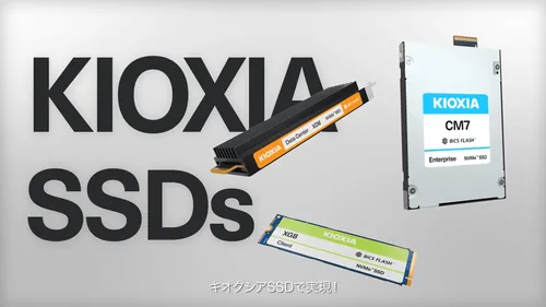
かつて、1TBのSSDが約1万円以下で手に入った時代は、静かに、しかし確実に幕を下ろしたようだ。 NAND型フラッシュメモリの発明者であり、業界の巨人であるキオクシア(旧東芝メモリ)から発せられた警告は、テクノロジー業界 […]
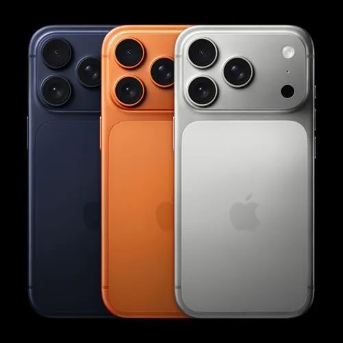
世界的な投資銀行であるMorgan Stanleyが実施した最新の台湾サプライチェーン調査は、テクノロジー業界に衝撃と安堵の両方をもたらす極めて興味深い事実を明らかにした。 2026年の市場投入が見込まれるiPhone( […]
2025年後半、世界の半導体メモリ市場で静かな、しかし大きな地殻変動が起きている。PCやスマートフォンのストレージとして不可欠な「NANDフラッシュメモリ」の価格が急騰。その背後には、Samsung Electronic […]
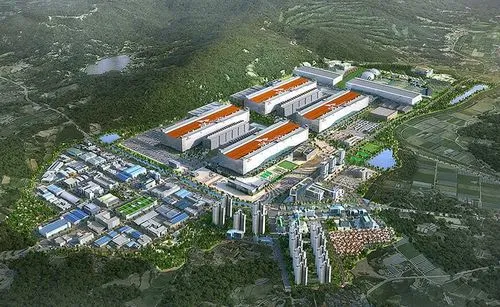
生成AIの爆発的な進化が、世界の産業構造を根底から揺さぶっている。その中心で今、最も激しい需給の嵐にさらされているのが、AIの頭脳を支えるメモリ半導体だ。この未曾有の需要を捉えるべく、韓国の半導体大手SK hynixが社 […]
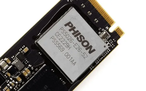
Windows 11 24H2向け累積更新プログラム「KB5063878」が、特定のNVMe SSDをシステムから消失させる深刻な不具合を引き起こしている問題で、大手SSDコントローラメーカーPhisonは遂に沈黙を破っ […]
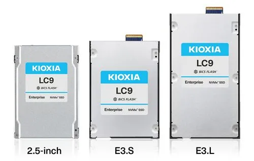
生成AIの進化が、データセンターの風景を根底から塗り替えようとしている。大規模言語モデル(LLM)や検索拡張生成(RAG)が要求するデータ量は天文学的に膨れ上がり、従来のストレージアーキテクチャは悲鳴を上げ始めた。こうし […]
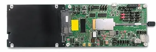
KIOXIAは、IOCore、京セラとの共同開発により、PCIe® 5.0インターフェースに対応した次世代の広帯域光SSDプロトタイプの動作確認に成功したと発表した。この技術は、最大40メートルという驚異的な長距離データ […]
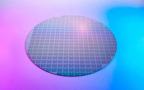
KIOXIAとSanDiskは、共同開発した第10世代3D NANDフラッシュメモリ技術を発表した。この新技術は、インターフェース速度、ビット密度、電力効率を大幅に向上させ、AI時代におけるデータストレージの進化を牽引す […]
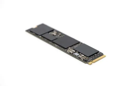
SanDiskは、PCIe Gen5の限界速度を達成しつつ、消費電力を7Wに抑えた新型SSDを発表した。2025年第2四半期に発売予定のこのドライブは、ゲーマーやOEMから高い評価を得ることが期待されている。 驚異的な速 […]
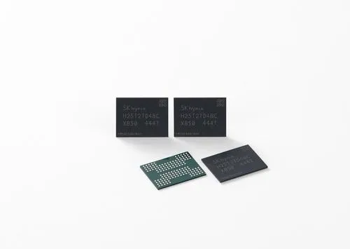
SK hynixは、世界初となる321層4D NANDフラッシュメモリの量産を開始したことを発表した。1テラビットの記憶容量を持つこの新製品は、独自の「3プラグ」製造プロセスを採用し、2025年上半期から顧客への出荷を開 […]
既にTrendForceの調査からもその兆しは見えていたが、SSD価格は安定するか、今後下落に向かいそうだ。NANDフラッシュメーカーのKioxiaに続き、SamsungやSK hynix等の他社もNANDフラッシュメモ […]
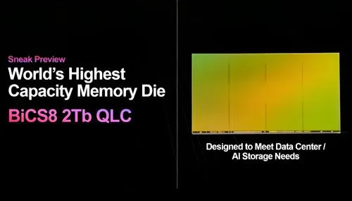
Western Digitalは最近開催した投資家向けプレゼンテーションの中で、世界初の2Tb 3Dクアッドレベルセル(QLC)NANDフラッシュメモリダイを発表した。このチップは、密度の点で競合他社を凌駕するものであり […]
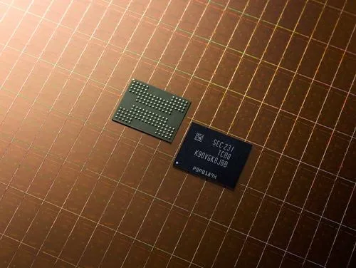
Samsungは、AI技術の高まりにより、高性能・大容量ストレージの需要が高まる中、競合他社に先んじて今月中に、290層の第9世代V-NAND(V9)チップの量産を開始する可能性があり、2025年には最大430層となる第 […]
The growth of the information and communication technology sector has vastly accelerated in recent decades because of advancements in digitalization and Artificial Intelligence (AI). Scope 1, 2, and 3 greenhouse gas emissions data of the top six semiconductor manufacturing companies (Samsung Electronics, Taiwan Semiconductor Manufacturing Corporation, Micron, SK Hynix, Kioxia, and Intel) were gathered from the publicly accessible Carbon Disclosure Project’s (CDP) website for 2020. Scope 3 emissions had the largest share in total annual emissions with an average share of 52%, followed by Scope 2 (32%) and Scope 1 (16%). Because of the absence of a standardized methodology for Scope 3 emissions estimation, each company used different methodologies that resulted in differences in emissions values. An analysis of the CDP reporting data did not reveal information on strategies implemented by companies to reduce Scope 3 emissions. The use of renewable energy certificates had the largest effect on decarbonization centered on reducing Scope 2 emissions, followed by the deployment of perfluorocarbon reduction technologies to help reduce Scope 1 fugitive emissions. Technology-specific marginal abatement costs of CO2 were also estimated and varied between −416 and 12,215 USD/t CO2 eq., which primarily varied depending on the technology deployed.
DRAM cell scaling down to the 14 nm design rule (D/R) has already been productized by major DRAM players such as Samsung, Micron, and SK Hynix. They’re developing n+1 (12~13 nm) and n+2 (11 nm or beyond) so-called D1b (D1β), D1c (D1γ), and D1d (D1δ) or even D0a generation now, which means DRAM cell D/R might be able to further scale down to single digit nm with EUVL adoption for DRAM cell/core patterning. The cell design scaling down is getting slower due to many scaling issues including patterning, leakage, and sensing margin. Major DRAM players have applied EUVL masks (such as SS_BLP/H_SC2) on DRAM and will expand it for the next generation. Current 6F2 cell architecture with 1T+1C will be moving over to 4F2 or 3D DRAM in an 8~9 nm D/R DRAM generation due to scaling limitations, which will be D0b or D0c. Although they change to 3D DRAM with a little relaxed CDs, EUVL will be a must for the performance and yield improvement (defects) in DRAM core areas such as very dense WLD and SA patterns just near the cell array. HKMG DRAM process has been adopted on Graphic DRAM and advanced DDR5 DRAM products by Samsung and Micron, although etching and high-k engineering are different for each. Major NAND manufacturers are still in the race to increase the number of vertical 3D NAND gates, they all have already introduced their own 176L/232L/238L 3D NAND devices. Samsung V-NAND, KIOXIA/WDC BiCS, Intel FG CuA, Micron CTF CuA, SK Hynix 4D PUC, and YMTC Xtacking 3D NAND products are the mainstream for SSD and mobile storage applications. Many innovative processes and designs have been adopted, however, lots of challenges are still there to overcome. Although lithography burdens were reduced by changing 2D to 3D, instead, UHAR etching/cleaning/filling-related developments are ongoing. Micron already exited XPoint memory, and Intel is winding it down as well. For SCM applications, fast NAND and some Emerging Memory (EM) devices such as Z-NAND, XL-FLASH, and STT-MRAM will cover the market needs in the future. Due to the difficulties of the EM materials etching, they’re currently limited to embedded and low-density applications only. We’ll discuss current and future challenges on DRAM, 3D NAND, and Emerging memory including process, design, and materials.
Ion beams have many applications. Junior Associate Professor Masahi Nojima, Research Institute of Science and Technology at the Tokyo University of Science, Japan, is working to create a new generation of ion beams. Already, he has successfully developed new techniques for producing focused ion beams (FIB). In his most recent work, Nojima has developed a metallic solution ion source that will be used to construct unknown functional materials by using ion beams made up of specific elements. The metallic solution ion source can generate a copy of an original structure using elementally selected materials. With support from the Japan Society for the Promotion of Science (JSPS), KAKENHI, the academic incentive system of the KIOXIA Corporation 2021 and the Toshiba Electric Devices & Storage Corporation 2021, Nojima is seeking to open up new materials for use as ion sources utilising electrospray ionisation (ESI) methods. By harnessing the elements of FIBs primarily created from liquid metal ion source (LMIS) by field ionisation processes, Nojima hopes to create new generations of ion beams. To date, he and the team have displayed the result of mass separating metallic ion solution ion beams on random conditions and, looking ahead, intend to estimate the stopping range of mass selected ion beams in solid materials.
In semiconductor manufacturing, major issues include automation of the operation, expansion of the production scale, and cost reduction and competitiveness enhancement by means of quality control. On Kioxia's production sites, a vast amount of data is collected from automated production lines. AI technologies are being applied to the data in order to implement information systems capable of quality monitoring and problem solving, which helps us keep high product quality. In this paper, three case studies of AI technology applications are reported. The first two cases are from the production stage, one being an application to yield analysis, and another being an application to defect inspection. The last case is from the design stage, an application to the topography simulation. On the other hand, the creation of artwork is a rapidly emerging field for the AI application. TEZUKA2020, a project in which AI and human collaboratively tried to produce a new piece of manga by the legendary Japanese artist Osamu Tezuka, was recently carried out as an ad campaign to promote Kioxia's corporate name. The project is briefly reported in this paper.