テクノロジー
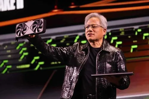
世界最大55万台のGPUを持つxAI、実は6万台分しか使えていないことが判明
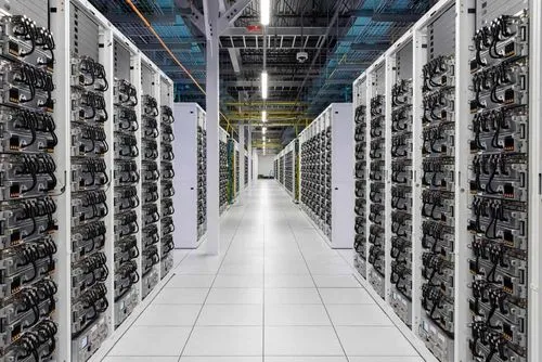
xAIは世界最大規模のAIクラスター「Colossus」を保有するが、その計算能力のわずか11%しか活用できておらず、新社長が2ヶ月以内に50%への改善を宣言した。これは、急速なハードウェア拡張に対しソフトウェア整備が追いつかず、MetaやGoogleに比べて実効的なGPU稼働率が著しく低いという構造的な課題を露呈している。
別名: NVLink
NVIDIAが開発した、GPU間を直接接続するための高帯域・低遅延な通信プロトコルおよびインターフェース。大規模なGPUクラスターにおいて、通信ボトルネックを解消しMFUを向上させるための鍵となる技術。
High performance multi-GPU computing becomes an inevitable trend due to the ever-increasing demand on computation capability in emerging domains such as deep learning, big data and planet-scale simulations. However, the lack of deep understanding on how modern GPUs can be connected and the real impact of state-of-the-art interconnect technology on multi-GPU application performance become a hurdle. In this paper, we fill the gap by conducting a thorough evaluation on five latest types of modern GPU interconnects: PCIe, NVLink-V1, NVLink-V2, NVLink-SLI and NVSwitch, from six high-end servers and HPC platforms: NVIDIA P100-DGX-1, V100-DGX-1, DGX-2, OLCF's SummitDev and Summit supercomputers, as well as an SLI-linked system with two NVIDIA Turing RTX-2080 GPUs. Based on the empirical evaluation, we have observed four new types of GPU communication network NUMA effects: three are triggered by NVLink's topology, connectivity and routing, while one is caused by PCIe chipset design issue. These observations indicate that, for an application running in a multi-GPU node, choosing the right GPU combination can impose considerable impact on GPU communication efficiency, as well as the application's overall performance. Our evaluation can be leveraged in building practical multi-GPU performance models, which are vital for GPU task allocation, scheduling and migration in a shared environment (e.g., AI cloud and HPC centers), as well as communication-oriented performance tuning.
NVLink-C2C is the enabler for Nvidia's Grace-Hopper and Grace Superchip systems, with 900GB/s link between Grace and Hopper, or between two Grace chips. The connection provides a unified, cache-coherent memory address space that combines system and HBM GPU memories for simplified programmability. This coherent, high-bandwidth, low-power, low latency connection between CPU and GPUs is key to accelerating the most complex AI and HPC workloads.
High-performance communication for very large messages on modern multi-GPU nodes has become increasingly important for Deep Learning workloads. These computing nodes are equipped with state-of-the-art interconnects, such as Nvidia's NVLink and PCIe, to facilitate communications between GPUs, and GPUs with the host processors. In this paper, we take on the challenge to design efficient intra-socket GPU-to-GPU communication using multiple NVLink channels at the UCX and MPI levels, and then utilise it to design an intra-node hierarchical NVLink/PCIe-aware GPU based MPI_Allreduce to enhance Horovod + TensorFlow with different models. UCX only utilises a small portion of the available NVLink bandwidth for intra-socket GPU-to-GPU communication. We propose a novel data transfer mechanism that stripes the message across multiple intra-socket communication channels and multiple memory regions using multiple GPU streams to utilise all available NVLink paths. Our approach achieves 1.69x and 1.84x higher bandwidth for UCX and Open MPI + UCX, respectively. We observe similar bandwidth improvements for large messages for MPI point-to-point communication when compared to other MPI implementations as they are also limited by data transfers by a single path. We then propose a 3-stage hierarchical, pipelined MPI_Allreduce design that incorporates the new multi-path NVLink data transfer mechanism for intra-socket communications in the first and third stages of the collective, and PCIe and X-bus channels for inter-socket GPU communication in the second stage with minimal interference. For large messages, our proposed algorithm achieves a high speedup when compared to Spectrum MPI, Open MPI + UCX, Open MPI + HPC-X, MVAPICH2-GDR, and NCCL. We also observe significant speedup for the proposed MPI_Allreduce for Horovod with TensorFlow with a variety of Deep Learning models.
Memory disaggregation decouples compute and memory resources, enabling efficient use of resources. Several interconnect technologies provide cache-coherent access to remote memory regions, which eases the use of disaggregated memory. Recent NVIDIA-based systems use the NVLink C2C interconnect, which provides cache-coherent memory access between CPUs and GPUs and their memory. While GPUs and NVLink are widely used to accelerate complex workloads, NVLink’s viability for connecting memory-expansion devices to a CPU remains unexplored. In this work, we quantify the characteristics of NVIDIA’s Grace CPU when accessing GPU memory via NVLink to assess NVLink’s viability for memory expansion. We benchmark throughput and latency for memory accesses on an NVIDIA Grace-Hopper system. We evaluate memory expansion when the CPU accesses both CPU and GPU memory and quantify the performance of database index operations with data stored in GPU memory. Our experiments show a throughput of up to 168 GB/s and access latencies between about 800 ns and 1000 ns.
xAIは世界最大規模のAIクラスター「Colossus」を保有するが、その計算能力のわずか11%しか活用できておらず、新社長が2ヶ月以内に50%への改善を宣言した。これは、急速なハードウェア拡張に対しソフトウェア整備が追いつかず、MetaやGoogleに比べて実効的なGPU稼働率が著しく低いという構造的な課題を露呈している。
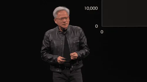
NVIDIAが発表した2026会計年度第4四半期(2025年11月〜2026年1月)決算は、同社がもはや単なる半導体メーカーではなく、次世代デジタル経済の基盤を完全に支配するインフラストラクチャー企業として君臨しているこ […]

NVIDIAによるAIインフラストラクチャへの支配力が、また新たな段階へと突入した。 2026年1月26日、NVIDIAはクラウドデータセンター事業者であるCoreWeaveに対し、新たに20億ドル(約3000億円規模) […]
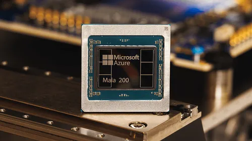
生成AIブームが「実験」のフェーズから「実装と運用」のフェーズへと移行する中、Microsoftがシリコンレベルでの巨大な賭けに出た。2026年1月27日、同社は自社開発の次世代AIアクセラレータ「Azure Maia […]
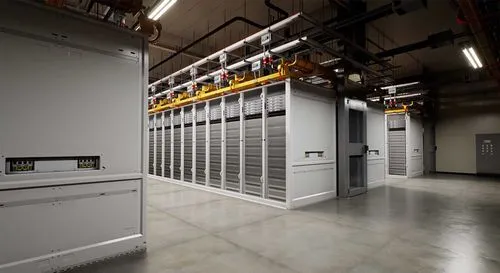
生成AI革命の裏側には、華々しいモデルの性能向上とは対照的な、泥臭く、過酷なハードウェアの現実が存在する。NVIDIA H100をはじめとする最新鋭GPUは、驚異的な演算能力を持つ反面、その運用は極めて不安定だ。 サーバ […]
AI(人工知能)革命を支える半導体市場において、長らく続いたNVIDIAの絶対的な支配体制に、今、大きな地殻変動の兆しが見える。既にAI時代の寵児であるOpenAIが、NVIDIAへの過度な依存からの脱却を目指し、長年の […]
PCI-SIGは、次世代インターコネクト規格「PCI Express 8.0」の仕様策定を開始したと発表した。2028年の仕様リリースを目指し、生データレート256.0 GT/s(ギガトランスファー/秒)、x16構成で1 […]
AI半導体市場を牽引するNVIDIAが、次世代の「Rubin」GPUプラットフォームにおいて、革新的なパッケージング技術「CoWoP(Chip-on-Wafer-on-PCB)」の採用を本格的に検討していることが、Dig […]
米国の厳格な輸出規制という逆風の中、半導体大手NVIDIAが中国市場向けに新たなAIチップを投入する計画であると、Reutersが報じている。最新のBlackwellアーキテクチャをベースとしつつも、性能と機能を大幅に絞 […]
NVIDIAは今後4年間で米国の半導体サプライチェーンに数千億ドルを投資する計画を発表した。同社CEO Jensen Huang氏は、全体で約5,000億ドル相当の電子機器を調達予定であり、そのうち「数千億ドル」を米国内 […]
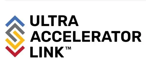
AMDやIntel、Meta、Microsoft、Googleなど9社のテクノロジー大手が、AI向けの新しい高速相互接続規格「Ultra Accelerator Link(UALink)」の標準化を目指すコンソーシアムを […]
MetaがLlama 3の大規模言語モデルのトレーニングを行う中で、NVIDIA H100 GPUの頻繁な故障に悩まされていたことが明らかになった。Metaが最近公開した研究によると、16,384基のNVIDIA H10 […]

AIアクセラレータ領域において、NVIDIAの支配は圧倒的だ。これに少しでも対抗しようと、先日Intel、Googleらは、CUDAプラットフォームからの脱却を目指したオープンソースのソフトウェア・スイートを開発する団体 […]
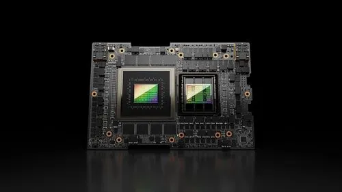
NVIDIAと言えば昔はゲーミングGPU、今はAI向けGPUでその名を轟かせているが、GPUのみならず、CPUとGPUを組み合わせた高性能コンピューティング(HPC)向けのスーパーコンチップも製造している。この、NVID […]
チップ設計の巨人であり現在はTenstorrentのCEOであるJim Keller氏は、NVIDIAが最近発表したBlackwell GPUアーキテクチャの研究開発費が100億ドルにも及んだことに対し、単に相互接続方式 […]

NVIDIAは、現行世代であるHopperアーキテクチャGPU「H100」と比較して最大5倍の性能向上を誇るという、次世代「Blackwell」アーキテクチャGPUと、それに基づくAIアクセラレータ「B200」GPUを正 […]