
テクノロジー
CFD、GIGABYTE製GPUの受注価格を8月分から改定へ:店頭価格への波及は未定
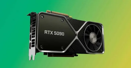
CFD販売がGIGABYTE製VGAの受注価格を8月1日分から現行価格比120〜140%へ改定すると告知。注文残のキャンセルにも触れ、GPU価格の上昇が店頭前の流通段階で表面化した。

グラフィックスカードやゲーム機などで広く採用されているビデオメモリ規格。GDDR7の登場により旧世代化しつつあるが、製造技術が確立されており供給が安定しているため、ミドルレンジ以下のGPUで引き続き重宝されている。
CFD販売がGIGABYTE製VGAの受注価格を8月1日分から現行価格比120〜140%へ改定すると告知。注文残のキャンセルにも触れ、GPU価格の上昇が店頭前の流通段階で表面化した。
AIサーバー向けメモリ需要の爆発的増加により、PC用GPUやVRAMの供給が深刻に停滞し、製品価格の高騰と市場の縮小を招いている。一方でCPUの供給は正常化へ向かっており、ベンダーは利益率重視の戦略へ転換することで収益の維持を図っている。
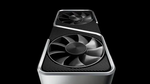
2026年1月5日、次世代GPUアーキテクチャ「Blackwell」を搭載したGeForce RTX 50シリーズの展開が本格化しようとするこのタイミングで、NVIDIAが2世代前の「Ampere」アーキテクチャ、GeF […]

Intelは次世代ゲーミングGPUとなるArcシリーズの新製品「Battlemage」を12月3日に正式発表することを明らかにした。当初2025年第1四半期での発売が予想されていた新製品の発表が前倒しされる形となり、PC […]
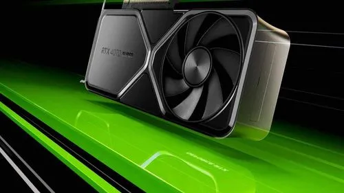
NVIDIAの信頼出来るリーカー、kopite7kimi氏によって次期「Blackwell」RTX 5000シリーズに搭載されるGPUファミリー「 GB202、GB203、GB205、GB206、GB207」の […]
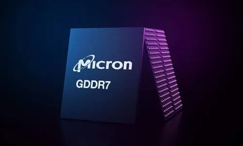
Micronは、次世代GDDR7メモリのサンプル出荷を開始した事を発表した。メモリ転送速度は実に32Gb/sとなり、帯域幅は1.5TB/sを実現するこのGDDR7は、GDDR6から最大60%の帯域幅向上を実現しており、N […]
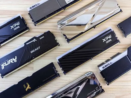
Microsoftのタスクマネージャーでは、現在メモリの速度は「MHz」表記が用いられている。これはメモリ業界が歴史的にこの指標を用いてきた名残からだが、最近のDDRメモリの速度にMHzを使用することが少なくなって来た業 […]
With advances in deep-neural-network applications the increasingly large data movement through memory channels is becoming inevitable: specifically, RNN and MLP applications are memory bound and the memory is the performance bottleneck [1]. DRAM featuring processing in memory (PIM) significantly reduces data movement [1]–[4], and the system performance is enhanced by the large internal parallel bank bandwidth. Among DRAM-based PIM proposals, [3] is near commercialization, but the required HBM technology may prevent it from being applied to other applications due to its high cost [5]. In this situation, an accelerator-in-memory (AiM) based on GDDR6 may be applicable: it has a relatively low-cost, is compatible with GDDR6 interface, and is designed to accelerate deep-learning (DL) applications. AiM offers a peak throughput of 1 TFLOPS with processing units (PUs) with a speed of 1 GHz utilizing the characteristics of GDDR6 with a speed of 16Gb/s. It can also support many applications as it has various activation functions. This paper first looks at the AiM architecture and the supported command set for DL operations. Next, the DL operations in the PU and supported activation functions are described. Finally, we present evaluation results of DL behavior of AiM at the package and the system level.
In this article, a 1.25-V 8-Gb, 16-Gb/s/pin GDDR6-based accelerator-in-memory (AiM) is presented. A dedicated command (CMD) set for deep learning (DL) is introduced to minimize latency when switching operation modes, and a bank-wide mantissa shift (BWMS) scheme is adopted to minimize calculation delay time, current consumption, and circuit area during multiply-accumulate (MAC) operation. By storing the lookup table (LUT) in the reserved word line in the dynamic random access memory (DRAM) bank cell, it is possible to support various activation functions (AFs), such as Gaussian error linear unit (GELU), sigmoid, and Tanh as well as rectified linear unit (ReLU) and Leaky ReLU. Performance evaluation was conducted by measuring the fabricated chip in ATE and a self-manufactured field-programmable gate array (FPGA)-based system. In the ATE-level evaluation, it operates at 16 Gbps up to a voltage as low as 1.10 V. When evaluated by GEMV and MNIST in the FPGA-based system, it was confirmed that the performance gains of 7.5–10.5 times were possible compared to the HBM2-based or GDDR6-based systems.
The demand for high-performance graphics systems used for artificial intelligence, cloud game, and virtual reality continues to grow; this trend requires graphics systems to achieve ever higher bandwidths. This article proposes a GDDR6 dynamic random access memory (DRAM) with a half-rate clocking architecture and optimized receiver and transmitter to improve high-speed operation. Furthermore, this article adopts a staggered PAD using the redistribution layer (RDL) to reduce the distance to four PADs; it enables the mitigation of bandwidth limitation of half-rate clocking, a lower phase mismatch, and a reduced propagation delay. The proposed half-rate clocking-based GDDR6 DRAM achieves 24 Gb/s/pin on a 1.35-V DRAM process. Also, the power-supply-induced-jitter (PSIJ) value is improved from 9.97 to 3.22 ps, compared to a GDDR6 design using a quarter-rate clocking. In addition, the phase mismatch of the proposed clock distribution network (CDN) is reduced compared to the conventional CDN, resulting in an improvement of the 3- $\sigma $ value of the phase skew from 4.16 to 2.25 ps.
This article introduces a 16-Gb T-coil-based graphics double-data-rate 6 (GDDR6) dynamic random access memory (DRAM) with merged-multiplexer (MUX) transmitter (TX), optimized data clock (WCK) operation to enhance I/O bandwidth. T-coil is implemented for the first time in a DRAM process. Moreover, an alternative-data-bus (ADB) is employed to solve the frequency limit of the data bus. The proposed T-coil-based GDDR6 DRAM achieves 27 Gb/s/pin with 1.35 V in a DRAM process.