
テクノロジー
GALAXが独立企業として解散、だがブランドは生き続ける:EVGA撤退との決定的な違いとは
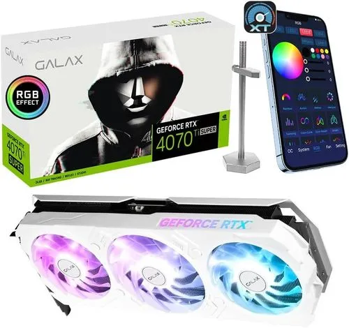
GPUメーカーGALAXが市場撤退したとの誤報が流れたが、実際は独立法人としての運営を終了し、ブランド管理が親会社Palit Groupに統合されたことが判明した。これは、GALAXのエンジニアチーム解散と香港オフィスの閉鎖を伴うものの、高性能GPUの開発・製造・サポートは継続され、ブランド自体は存続する戦略的移行である。

別名: GDDR7
GDDR7(Graphics Double Data Rate 7)は、グラフィックス処理ユニット(GPU)向けに設計された高帯域幅メモリの規格であり、GDDR6/GDDR6Xの後継に位置づけられる。高解像度ゲーミングやAI推論など、大容量かつ高速なメモリ帯域幅を必要とする用途に対応することを目的として策定されている。
GDDR7は、従来のGDDR6世代と比較してデータ転送速度やメモリ帯域幅の大幅な向上を目指した規格だ。GPUにおけるメモリはレンダリングパフォーマンスや機械学習の推論速度に直結するため、各世代の規格更新はシステム全体の性能向上に大きく寄与する。また、コンシューマー向けゲーミングGPUのみならず、ゲームコンソールやプロフェッショナル向けアクセラレータへの搭載も視野に入れられている。
2026年5月時点で流通した情報によれば、ソニーの次世代ゲームコンソール「PlayStation 6」には30GBのGDDR7メモリが搭載される可能性があると、信頼性の高いリーク情報源として知られるKepler_L2氏が報告している。PlayStation 5の発売から約5年が経過したこのタイミングで、次世代機に向けたメモリ規格としてGDDR7が有力候補として浮上している形だ。一方、2026年6月に報じられた記事では、AIブームによる半導体資源の逼迫が次世代ゲームハードウェアの開発スケジュールに影響を及ぼしており、PS6の発売が2029年へ後ろ倒しになる可能性も指摘されている。
NVIDIAのGPU市場においては、AI需要の急増によりゲーミング向けGPUの供給が圧迫されているとの報道が2026年に相次いだ。同社のAICパートナーへの供給が約20%削減されるとの観測や、2026年を通じて新たなゲーミングGPUが投入されない可能性が伝えられており、次世代GPU「RTX 60シリーズ」は2027年後半以降にずれ込むとの見方も出ている。こうした状況は、GDDR7を採用する次世代製品の市場投入タイミングにも影響を及ぼし得る。
新興GPU企業であるBolt Graphicsは、2026年6月に高性能GPU「Zeus」のテストチップのテープアウトを完了したと発表したが、量産時期は当初の2026年後半から2027年第4四半期へと後ろ倒しとなった。こうした事例は、最新メモリ規格を採用した高性能GPUの開発・量産がいかに困難なフェーズにあるかを示している。
AI需要による半導体リソースの争奪は、GDDR7を含む先端メモリの生産リソースにも影響を与えている。ゲーミング向けGPUの開発スケジュールが後ろ倒しになる中、GDDR7搭載製品の本格的な普及も従来の予測よりも遅延する可能性がある。一方で、次世代コンソールへの採用が現実味を帯びてきたことで、コンシューマー市場でのGDDR7普及に向けた動きは着実に進んでいるとみられる。
GPUメーカーGALAXが市場撤退したとの誤報が流れたが、実際は独立法人としての運営を終了し、ブランド管理が親会社Palit Groupに統合されたことが判明した。これは、GALAXのエンジニアチーム解散と香港オフィスの閉鎖を伴うものの、高性能GPUの開発・製造・サポートは継続され、ブランド自体は存続する戦略的移行である。
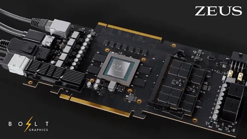
Bolt Graphicsは高性能GPU「Zeus」のテストチップのテープアウトに到達したが、量産時期は初期告知の2026年後半から2027年第4四半期へと後ろ倒しになった。このテープアウトは設計の前進を示すものの、実性能や量産を保証するものではなく、今後の実測値や事業化の進展が注目される。

2026年、ゲーム業界はかつてない「ハードウェアの壁」に直面している。長年、コンソール市場を牽引してきた「数年おきに性能を倍加させ、手頃な価格で提供する」というビジネスモデルが、シリコンバレーで巻き起こった空前絶後のAI […]

PlayStation 5の発売から約5年が経過し、ゲーム業界の視線はすでに「次」へと向いている。長年信頼性の高いリーク情報を発信してきた実績を持つKepler_L2氏による最新の情報では、次世代コンソールであるPlay […]

NVIDIAが、2026年におけるゲーミング用新型GPUの投入を一切見送る方針を固めたことが明らかになった。同社が1年を通じてゲーミング向けの新製品を1つもリリースしないのは、1990年代半ば以来、実に約30年ぶりの異常 […]
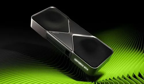
現代のデジタルエコシステムにおいて、GPU(Graphics Processing Unit)は単なる画像処理装置の枠を超え、世界経済を牽引する戦略物資としての地位を確立している。しかし今、PCゲーマーやシステムビルダー […]
PCゲーマーにとって、2026年の幕開けは寂しい物になった。ラスベガスで開催されたCES 2026において、多くのゲーマーやエンスージアストが期待していたNVIDIAからの「次の一手」――すなわちGeForce RTX […]
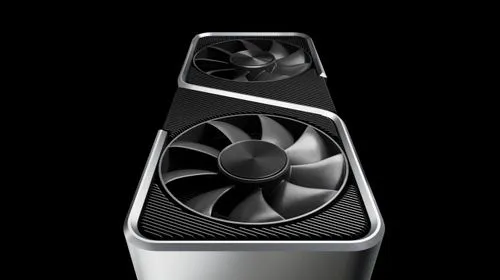
2026年1月5日、次世代GPUアーキテクチャ「Blackwell」を搭載したGeForce RTX 50シリーズの展開が本格化しようとするこのタイミングで、NVIDIAが2世代前の「Ampere」アーキテクチャ、GeF […]
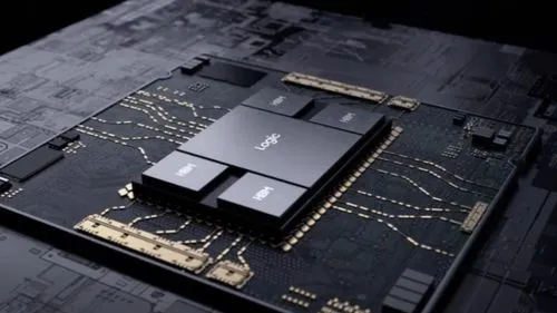
2025年12月11日、JEDEC(半導体技術協会)が、次世代メモリ規格「SPHBM4(Standard Package High Bandwidth Memory)」の開発が完了間近であると発表した。 AI(人工知能) […]

半導体業界、特にメモリ市場において、直感に反する劇的なパラダイムシフトが進行している。世界中の注目がAI専用メモリである「HBM(High Bandwidth Memory)」に注がれる中、メモリ界の巨人Samsung […]
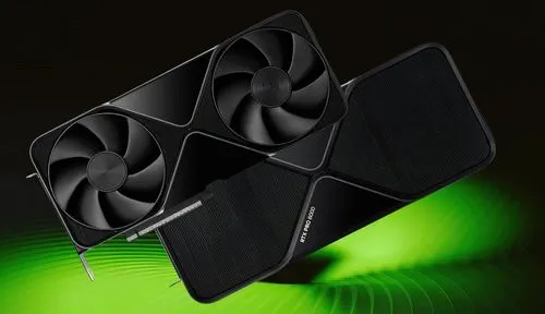
テクノロジー業界の深層において、地殻変動にも似た静かなる異変が起きている。世界的なAIブームが半導体市場をかつてない活況へと導く一方で、その「光」の裏側で、ゲーミンググラフィックボード(GPU)市場に深刻な「影」が落ちつ […]
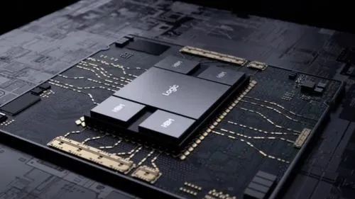
Samsung Electronicsが2025年10月30日に発表した第3四半期決算は、市場の予想を上回る好調な内容であった。しかし、その数字の羅列の奥で、テクノロジー業界の未来を占う極めて重要なマイルストーンが示され […]

AI革命の波が、半導体市場の根幹を揺さぶり始めた。韓国メディアの報道によると、メモリ半導体の世界最大手であるSamsung ElectronicsとSK hynixが、2025年第4四半期に向けてDRAMおよびNANDフ […]
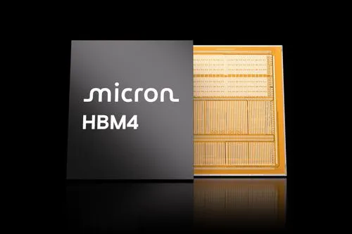
AI(人工知能)の進化が世界のテクノロジー地図を塗り替える中、その心臓部である半導体の性能競争は新たな次元に突入している。この競争の鍵を握るのが、プロセッサにデータを供給する「メモリ」の存在だ。米半導体大手Micron […]
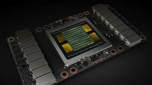
米国の厳格な輸出規制という逆風の中、半導体大手NVIDIAが中国市場向けに新たなAIチップを投入する計画であると、Reutersが報じている。最新のBlackwellアーキテクチャをベースとしつつも、性能と機能を大幅に絞 […]
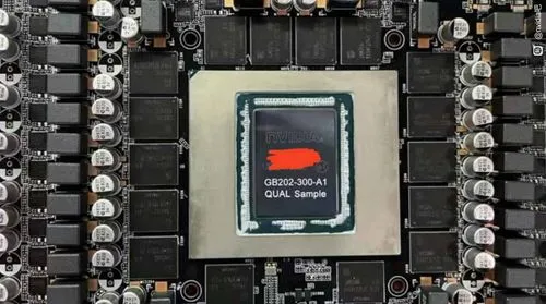
NVIDIAの次世代ゲーミングフラグシップGPU「GeForce RTX 5090」のPCB(プリント基板)とされる画像が中国のテクノロジーフォーラムでリークされた。画像からは、大型のGB202 “Black […]

次世代GPUとなるNVIDIA GeForce RTX 5090および5080を搭載したAcer Predator Orion 7000シリーズの価格情報が、ドイツの小売店サイトに誤って掲載され、大きな話題となっている。 […]
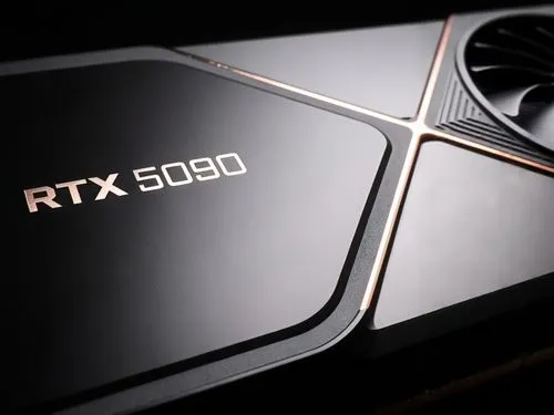
NVIDIAの次世代フラッグシップGPU「GeForce RTX 5090」に搭載されるGB202チップが、744平方ミリメートルという巨大なダイサイズを持つことが明らかになった。これは現行のRTX 4090のAD102 […]
NVIDIAの信頼出来るリーカー、kopite7kimi氏によって次期「Blackwell」RTX 5000シリーズに搭載されるGPUファミリー「 GB202、GB203、GB205、GB206、GB207」の […]
NVIDIAの次世代GeForce RTX 5000シリーズ(Blackwell)のノートPC向け製品の一部情報がリークされ、そのメモリ構成などの詳細情報が明らかとなった。この情報はノートPCを製造する台湾のOEM及びO […]
The increase in GPU-based AI applications, cloud-based gaming, and video streaming services has driven the need for new a graphics memory that operates at higher bandwidth and power efficiency than existing GDDR6 SDRAM, leading to the introduction of the GDDR7 standard [1]. Since performance degradation due to thermal throttling, power cost, and device reliability are major development considerations in high-power graphics applications, PAM3 signaling is applied on single-ended pins to improve bandwidth and power consumption, while maintaining the clock frequency [2]. However, new PAM3-related blocks supporting double the bandwidth inevitably increase in absolute power and temperature. In this paper, we present additional power reduction techniques, while maintaining SNR. The clocking architecture, with fast wake-up capabilities, can be partially disabled to provide active-standby current (IDD3N) as low as the power-down mode. The PAM3 TX and RX use a design approach that achieves high SNR and power efficiency.
The development of the graphics double-data-rate 7 (GDDR7) dynamic random access memory (DRAM) standard aims to overcome the constraints of its predecessor, GDDR6, in order to achieve higher speed operation. This article introduces a 16-Gb GDDR7 DRAM with three-level pulse amplitude modulation (PAM3) interface in a DRAM process. The proposed GDDR7 consists of two dies/four channels to support both two- and four-channel mode configuration. An adaptive gain-controlled feedforward equalizer (FFE) is implemented in the transmitter (TX) and data-dependent separately gain-controlled one-tap decision feedback equalizer (DFE) is proposed in the receiver (RX). In addition, the proposed ZQ calibration scheme uses alternately switched reference voltages to enhance the level mismatch ratio (RLM) of the PAM3 signaling. Moreover, low-power and low-jitter clocking techniques with a low-dropout (LDO) regulator and CMOS distribution are employed for WCK distribution; thereby, 60 mA per die of current reduction and 0.16 ps/mV of power-supply-induced jitter (PSIJ) could be achieved. The proposed GDDR7 achieves 37 Gb/s at 1.2 V and 32 Gb/s at 1.1 V with a 1z-nm DRAM technology.
This paper presents a 40-Gb/s/pin single-ended PAM-4 transceiver for GDDR7. LV-POD interface that separates the internal voltage from the channel supply voltage (VDDQL) is used to reduce channel power consumption. Direct 4-tap decision feedback equalizer (DFE) with timing calibrated reset-less slicer at receiver (RX) and asymmetric bidirectional T-coil are employed to achieve the highest data-rate among the state-of-the-art DRAM I/Os. The prototype chip is fabricated in mimicked 10-nm class DRAM process using 28-nm CMOS. At sub-1V VDDQL, measured TX common eye window is 0.31UI. Measured RX shmoo has total of 162 pass ticks, each tick with the size of 5mV * 1ps and BER under 10-6. The total energy efficiency of 2.02pJ/b was achieved.
Demand for high-bandwidth graphics memory is rapidly increasing for various applications such as AI, deep learning, autonomous cars, etc. To meet this demand, $\text{GDDR}6\mathrm{X}$ uses multilevel signaling (PAM4) for the first time in DRAM [1], while GDDR7 targets data-rates $28\text{Gb}/\mathrm{s}$ or higher using PAM3 signaling. However, the increased data rate incurs higher inter-symbol interference (ISI), while PAM3 is more vulnerable to ISI than PAM2 signaling. Decision feedback equalizers (DFEs) are widely used in receivers (RX) to remove post-cursor ISI without amplifying noise. A PAM3 RX, with an analog DFE, typically employs a direct feedback (DF) implementation, which must meet stringent feedback timing requirements. As the target speed increases it is challenging to reduce the feedback time to within 1 unit interval (UI) for a PAM3 RX due to the increased line parasitics and gate loading. While the loop-unrolled (LU) DFE technique mitigates feedback timing constraints, implementing a PAM3 LU DFE results in additional area and power overhead. In view of these drawbacks, this paper proposes a new type of PAM3 DFE, which combines the qualities of DF and LU DFEs to minimize area and power overhead, while also reducing the feedback time.
The trend of multi-chip modules (MCMs), die-to-die (D2D), and chiplet interfaces (e.g. UCIe) requires high-bandwidth densities while minimizing power consumption [1], [3], [4], [11]–[13]. Single-ended (SE) PAM3 signaling has been adopted in GDDR7 [2] as a high-bandwidth solution, increasing the data rate by 150%, compared to NRZ (PAM2) using the same baud rate. SE PAM3 signaling can also be applied to chiplet interfaces, but it faces challenges (Fig. 22.1.1): (1) the RX requires large-area reference-voltage $(\mathrm{V}_{\text{refp}}$ & $\mathrm{V}_{\text{refn}})$ generators. (2) Matching RX and TX references is challenging, and discrepancies result in a TX-RX reference offset. (3) TX drivers generate simultaneous switching noise (SSN) of up to a few hundred millivolts on $\mathrm{V}_{\text{DI}}$ in TX die [3]; this noise coupled to TX data and cannot be rejected by the RX, thereby degrading voltage margins. (4) Reducing channel pitch increases crosstalk, and PAM3 is $2\times$ more vulnerable to crosstalk than NRZ.